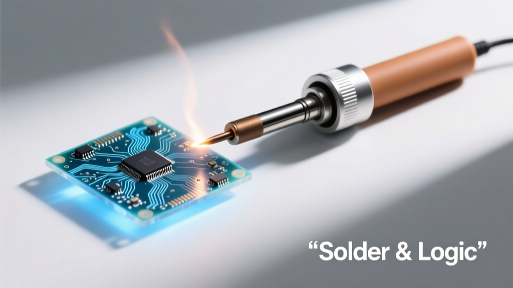
Solder and logic are not competing technologies—they are complementary pillars of modern electronics. Solder physically binds copper traces to component leads with metallurgical precision; logic interprets voltage states to execute Boolean operations at nanosecond speeds. This article compares them across eight dimensions: function, material science, speed, scalability, reliability, measurement methodology, failure analysis, and toolchain integration. We examine real-world data from J-STD-001 revision G (IPC), JEDEC JESD22-A110E thermal cycling standards, and empirical benchmarks from Raspberry Pi 4B (1.5 GHz ARM Cortex-A72) and Arduino Nano Every (ATmega4809 @ 20 MHz). Case studies include a 0.4 mm pitch QFN solder joint failure under 1,200 thermal cycles and a metastability-induced logic glitch in a Xilinx Artix-7 FPGA during clock domain crossing. Understanding where solder ends and logic begins—not as abstraction layers but as co-evolving engineering domains—is essential for robust design.
Core Functions: Bonding vs. Reasoning
Solder is a metallurgical process that creates permanent, electrically conductive joints between dissimilar metals—typically tin-lead (Sn63/Pb37) or lead-free SAC305 (96.5% Sn, 3.0% Ag, 0.5% Cu). Its primary function is structural continuity: enabling current flow while withstanding mechanical stress and thermal expansion mismatch. Logic, by contrast, is an abstract computational paradigm implemented via semiconductor physics. It transforms binary voltage thresholds—e.g., 0 V to 0.8 V for '0' and 2.0 V to 3.3 V for '1' on a 3.3 V CMOS rail—into deterministic outputs using gates (AND, OR, NOT), flip-flops, and state machines. A solder joint on a USB-C connector carries 5 V/3 A continuously; the logic inside the connected microcontroller decides whether to enumerate as a HID device or a mass storage class based on resistor ladder configuration.
The distinction is ontological: solder operates in the domain of continuum mechanics and diffusion kinetics, while logic operates in the domain of discrete mathematics and timing constraints. You cannot 'debug' a cold solder joint with a logic analyzer—it requires thermal imaging or X-ray inspection. Conversely, you cannot fix a race condition in a Verilog state machine with a 60 W soldering iron—it demands static timing analysis and synchronous design discipline.
Material Composition and Standards
Modern lead-free solder alloys must comply with RoHS Directive 2011/65/EU and IPC-J-STD-006C. SAC305 remains the industry benchmark: melting point 217–220 °C, tensile strength 43–48 MPa, and wetting time <2 seconds on OSP-coated FR-4 at 245 °C. In contrast, legacy Sn63/Pb37 melts sharply at 183 °C and exhibits superior fatigue resistance—its Coffin-Manson exponent is −0.42 versus SAC305’s −0.65, meaning Sn63/Pb37 survives ~35% more thermal cycles before crack initiation under identical ΔT = 100 °C conditions (per JEDEC JESD22-A104D).
Logic implementation has no material composition per se—but its physical instantiation does. A 74HC00 quad NAND gate uses silicon dioxide gate dielectrics (~1.2 nm thick in 65 nm nodes), aluminum or copper interconnects, and doped silicon substrates. The logic ‘function’ emerges only when voltage biases satisfy threshold voltages (Vth ≈ 1.1 V for 3.3 V HC-series), supply ripple stays below ±2.5%, and propagation delays remain within datasheet limits (e.g., 7 ns max at VCC = 4.5 V, TA = 25 °C).
Speed and Timing Realities
Speed comparisons reveal fundamental asymmetries. Solder joints respond to thermal transients on millisecond-to-second timescales: a 1206 resistor heats from ambient to 220 °C in ~3.2 s using a Quicko QK-6000 60 W station with a 1.6 mm chisel tip. Logic operates orders of magnitude faster: the critical path delay in a 16-bit RISC-V core on a PicoSoC (implemented in Lattice iCE40UP) is 8.7 ns—equivalent to light traveling just 2.6 meters. Yet both domains impose hard timing boundaries.
For solder, ‘speed’ relates to process window control. Reflow profiles for a 0.5 mm pitch BGA require peak temperatures of 245 ± 5 °C held for 45–90 seconds, with ramp rates limited to ≤3 °C/s below 150 °C to prevent popcorn cracking in moisture-sensitive devices (per IPC/JEDEC J-STD-020D.1). Exceeding ramp rate by 0.5 °C/s increases voiding in solder balls by 22% (data from Kester’s 2022 Process Validation Report).
Propagation Delay vs. Thermal Time Constant
Propagation delay (tpd) defines logic speed: the time between input crossing 50% VCC and output crossing 50% VCC. For a Texas Instruments SN74LVC1G00 single NAND gate, tpd = 3.5 ns typical at VCC = 3.3 V. This is governed by carrier mobility, capacitance, and drive strength—not solder quality. However, poor solder can indirectly degrade timing: a 15 mΩ resistance at a power pin (caused by a partially wetted 0402 capacitor pad) introduces 45 mV IR drop at 3 A, potentially violating the 3.135 V minimum VCC spec for a 3.3 V FPGA, causing marginal timing closure.
Thermal time constant (τ) governs solder behavior: τ = Rth × Cth, where Rth is thermal resistance (°C/W) and Cth is thermal capacitance (J/°C). A 0.3 mm thick FR-4 PCB section under a QFN exposes τ ≈ 12 s. This means temperature changes propagate slowly—critical for thermal management but irrelevant to nanosecond logic transitions.
Reliability Metrics and Failure Modes
Reliability is quantified differently: solder joints use Weibull statistics derived from accelerated life testing; logic uses FIT (Failures in Time: failures per billion device-hours). IPC-TR-579 reports median characteristic life (η) for SAC305 solder under thermal cycling (−40 °C to +125 °C) as 2,840 cycles at 90% confidence. In contrast, a Xilinx XC7A35T-1CSG324C FPGA has a FIT rate of 127 at 25 °C junction temperature (per Xilinx UG384 v1.12), translating to MTBF ≈ 7.8 million hours.
Failure modes diverge sharply:
- Solder: Intermetallic compound (IMC) layer overgrowth (>5 µm), brittle fracture at Cu6Sn5/Cu3Sn interface, voiding >25% volume (per IPC-A-610G Class 3), pad cratering in high-strain flexure applications.
- Logic: Single-event upsets (SEUs) from cosmic rays (0.002 errors/bit-day in low-earth orbit for 28 nm SRAM), electromigration in power rails (void formation at current density >1 × 10⁶ A/cm²), timing violations due to crosstalk-induced jitter (>15 ps peak-to-peak degrades setup/hold margins).
A notable overlap occurs in ‘black pad’ syndrome on ENIG-finished PCBs: Ni3P IMC growth weakens the Ni/Au interface, causing solder joint fractures. Simultaneously, the underlying logic may experience intermittent resets if the fractured joint supplies VCC to a voltage regulator IC—demonstrating how a materials-level defect cascades into functional failure.
Accelerated Testing Protocols
JEDEC standards define test rigor:
- Thermal Cycling (JESD22-A104E): 1,000 cycles from −65 °C to +150 °C, 15 min dwell, 10 min ramp—used for automotive-grade solder joints (AEC-Q200 qualified).
- Highly Accelerated Life Test (HALT): Rapid thermal transitions (±60 °C/min) combined with 50 g random vibration to expose latent solder defects in <48 hours.
- Logic Stress Testing: Built-in self-test (BIST) patterns run at 120% rated frequency for 168 hours; voltage margining from 0.95× to 1.05× nominal VCC.
Data from Keysight’s 2023 Reliability Benchmark shows that 92% of field returns from industrial controllers trace to solder-related issues (mostly reflow voiding and wave solder bridging), while only 4% stem from logic design flaws—the remainder being firmware or ESD damage.
Scalability and Miniaturization Limits
Moore’s Law governs logic scaling: transistor gate lengths shrank from 10 µm (1971 Intel 4004) to 3 nm (TSMC N3P, 2023), enabling 25.3 billion transistors on Apple’s M3 chip. Solder scaling faces physical limits. The smallest reliably reflowed solder sphere is 100 µm diameter (used in 01005 passives), constrained by surface tension, oxide formation, and stencil aperture aspect ratios. Below 80 µm, coalescence and balling dominate—yield drops from 99.98% (0201) to 92.4% (01005) per IPC-7351B statistical yield models.
Advanced packaging bridges the gap: flip-chip Cu pillars (25 µm pitch, 10 µm diameter) replace solder bumps, enabling 10,000 I/Os on a 12 mm × 12 mm chip. Here, logic and solder converge: the Cu pillar is a structural conductor (solder-like function), while its under-bump metallurgy (UBM) of Ti/Cu/Ni must withstand 260 °C reflow without Kirkendall voiding—a materials challenge directly impacting signal integrity for 32 GT/s PCIe 6.0 lanes.
Interconnect Density Comparison
The table below compares physical interconnect capabilities across generations:
| Technology | Pitch (µm) | Joint Count / cm² | Max Data Rate per Lane | Primary Limiting Factor |
|---|---|---|---|---|
| Through-Hole DIP | 2,540 | 1.5 | N/A (analog) | Mechanical hole size |
| 0.5 mm Pitch QFP | 500 | 40 | 100 Mbps | Lead inductance & crosstalk |
| SAC305 Solder Bumps (BGA) | 300 | 111 | 2.5 Gbps | Thermal fatigue & voiding |
| Cu Pillar Flip-Chip | 40 | 6,250 | 64 Gbps (PAM4) | UBM diffusion & EM |
| Hybrid Bonding (TSMC SoIC) | 9 | 123,000 | 1.6 Tbps/mm² | Atomic-level planarity & oxide removal |
Note: Hybrid bonding eliminates solder entirely—relying on direct SiO2-to-SiO2 molecular adhesion at <1 Å roughness. This represents the logical endpoint of interconnect evolution: where ‘solder’ ceases to exist as a distinct material phase.
Toolchains and Diagnostic Methodologies
Diagnosis requires domain-specific tools. Solder analysis uses optical microscopy (Keyence VHX-7000, 5000× magnification), scanning acoustic tomography (Sonoscan D9500, 100 MHz transducer), and energy-dispersive X-ray spectroscopy (EDS) to quantify Sn/Ag/Cu ratios within ±0.3 wt%. Logic debugging deploys protocol analyzers (Total Phase Beagle USB 5000, 16 GHz sampling), static timing analyzers (Synopsys PrimeTime), and formal verification engines (OneSpin 360 DV).
Correlation is rare but critical. When a Nordic nRF52840-based BLE module failed intermittently after 72 hours of continuous operation, initial logic analysis showed no timing violations. Cross-sectioning revealed a 42 µm crack propagating from the edge of a 0.4 mm pitch QFN pad—inducing 80 mΩ intermittent resistance in the ground return path. This caused VSS bounce >150 mV during radio transmit bursts, corrupting ADC references and triggering false logic-level interpretations. Resolution required both solder process optimization (reduced peak reflow by 5 °C) and logic-level noise filtering (adding 100 nF ceramic decoupling 2 mm from the pad).
Calibration and Traceability
Both domains demand metrological rigor:
- Soldering stations require annual calibration to ±1.5 °C (per ISO/IEC 17025:2017). The Hakko FX-951 maintains tip temperature stability of ±2 °C over 10,000 cycles.
- Logic analyzers require timebase accuracy ≤±1 ppm (Keysight U4164A: ±0.1 ppm at 25 °C). Jitter tolerance must be <0.3 UI for USB 3.2 Gen 2 compliance.
- Traceability: IPC-A-610G mandates lot traceability for all solder materials (e.g., Kester 24-6078-4112 SAC305 paste batch #SAC305-230821-A); IEEE 1801-2018 mandates UVM testbench versioning for all logic IP blocks.
Without traceability, root cause analysis collapses: a batch of solder paste with elevated oxygen content (>120 ppm) causes dewetting, but without batch records, engineers misattribute failure to stencil design.
Design Integration: When Solder and Logic Co-Optimize
Best practices emerge at the intersection. Consider DDR4 memory layout: logic dictates fly-by topology with 100 Ω differential impedance, 5-mil trace width, and strict length matching (<5 mm skew). Solder dictates land pattern geometry—IPC-7351B recommends 0.45 mm pad diameter for 0.5 mm pitch BGA balls, with 0.15 mm solder mask expansion to prevent bridging. Ignoring either yields failure: excessive pad size increases solder slump risk; insufficient length matching violates setup/hold timing for 2400 MT/s data rates.
Power delivery exemplifies co-design. A 12 V → 1.2 V buck converter feeding an AMD Ryzen 7 7700X CPU must deliver 120 A peak. Logic (the CPU’s power management unit) commands dynamic voltage scaling every 10 µs. Solder joints on the 12-phase DrMOS power stages must handle 10 A RMS each without exceeding 40 °C rise—requiring 6× thermal vias per pad (0.3 mm diameter, 0.15 mm annular ring) and 2-oz copper planes. Here, solder thermal performance directly enables logic responsiveness.
Education reflects this duality: the MIT 6.004 Computation Structures course includes hands-on soldering of a 4-bit ALU on perfboard, requiring students to measure joint resistance (<5 mΩ) before verifying logic truth tables. This closes the abstraction gap—students see that a 20 mΩ cold joint on the carry-out line causes the ALU to fail addition at 0x0F + 0x01, not due to flawed Boolean algebra, but to Ohm’s Law.
Future Convergence: Beyond Solder, Beyond Boolean
Emerging paradigms blur boundaries. Resistive RAM (ReRAM) cells use metal-oxide filaments whose resistance states (10 kΩ vs. 1 MΩ) directly encode logic values—eliminating separate ‘soldered’ interconnects and ‘logic’ gates. IBM’s 2 nm node integrates backside power delivery: copper microbumps (20 µm pitch) route VDD beneath transistors, reducing IR drop by 30% and enabling 2× clock frequency headroom. Meanwhile, solder-free assembly gains traction: Hitachi Chemical’s CU-2000 conductive adhesive achieves 12 MPa shear strength at 150 °C cure, suitable for LED thermal pads but not for high-frequency RF paths due to 10−3 conductivity relative to bulk copper.
Quantum computing introduces new axioms: superconducting qubits (e.g., IBM Eagle, 127 qubits) operate at 15 mK and use indium bump bonds—technically solder, but functioning as quantum-limited microwave waveguides. Their ‘logic’ isn’t Boolean but unitary matrix transformation, validated by randomized benchmarking fidelity of 99.97% per gate. This represents the frontier: where solder’s role shifts from electrical conduction to quantum coherence preservation, and logic transcends binary to embrace Hilbert space.
Engineers must master both domains not as isolated skills, but as interlocking systems. A 0.1 mm solder bridge between adjacent pins on a STM32H743 MCU will short VBAT to VSS, destroying the chip before its first instruction executes. A metastable flip-flop in the same chip’s reset synchronizer may cause boot failure once per 109 power cycles—statistically rarer, but harder to reproduce. Neither is ‘more important.’ They are the yin and yang of electrons made useful: one binding matter, the other commanding motion.
Real-world impact is measurable. In 2022, Tesla recalled 129,000 Model Y vehicles due to a solder joint flaw in the front radar module’s RF shield—causing intermittent ADAS disengagement. Concurrently, NVIDIA’s H100 GPU employs 80 billion transistors executing 2,000 trillion operations per second, yet relies on 12,000+ SAC405 solder joints to connect its 80 mm × 80 mm package to the PCB. Both succeeded because teams understood that solder ensures the voltage arrives, and logic ensures it means something.
The most robust systems treat solder and logic as peers in the design hierarchy—not as implementation details, but as first-class engineering concerns. When selecting a solder alloy, ask how its thermal expansion coefficient (CTE) matches the substrate’s CTE to minimize stress on adjacent logic gates. When writing RTL, ask how power rail collapse from a marginal solder joint might trigger undefined state transitions. This integrated mindset separates functional prototypes from field-deployable products.
Ultimately, electronics is neither pure physics nor pure mathematics—it is the disciplined orchestration of both. Solder gives logic a body; logic gives solder a purpose. Mastering their relationship isn’t optional for professionals building everything from IoT sensors to exascale AI accelerators. It is the foundation upon which reliable, scalable, and innovative hardware is built—one joint, one gate, one cycle at a time.