
The Metallurgy of Failure: Inside a Soldering Cold Joint
In high-reliability electronics manufacturing, a soldering cold joint is far more than a cosmetic blemish. It represents a critical point of failure that can compromise automotive engine control units (ECUs), aerospace flight controllers, and medical life-support systems. Unlike a pristine metallurgical bond, a cold joint exhibits high electrical resistance, severe mechanical fragility, and a high susceptibility to thermal fatigue and vibration-induced fracturing.
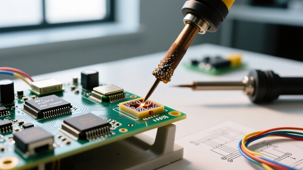
To understand why a soldering cold joint fails, we must look at the microstructural level. A proper solder connection relies on the formation of an Intermetallic Compound (IMC) layer—typically Cu6Sn5 when using SnPb or SAC305 (Lead-Free) alloys on copper pads. This IMC layer should be uniformly 1 to 3 microns thick. When thermal energy is insufficient during the reflow or hand-soldering process, the solder paste melts physically but fails to achieve the activation energy required for atomic diffusion. The result is a cold joint: a mechanical wrap rather than a true metallurgical weld, characterized by a dull, grainy, and convex appearance.
IPC-A-610 Defect Classifications
The IPC (Association Connecting Electronics Industries) provides the definitive framework for evaluating solder quality in the IPC-A-610 standard. Understanding how inspectors classify a soldering cold joint is essential for quality control engineers and manufacturing managers.
| IPC Class | Target Application | Cold Joint Criteria (Defect) | Acceptance Tolerance |
|---|---|---|---|
| Class 1 | General Consumer Electronics | Dull, grainy, or fractured appearance; poor wetting. | Must maintain electrical continuity; mechanical strength is secondary. |
| Class 2 | Dedicated Service Electronics (IT, Comms) | Any visible evidence of disturbed or cold solder; incomplete wetting. | Zero tolerance for cold joints on high-stress or high-current joints. |
| Class 3 | High-Performance / Aerospace / Medical | Any joint lacking a smooth, shiny, concave fillet; grainy texture. | Strict rejection. A single soldering cold joint mandates board-level rework. |
Root Causes in High-Volume Manufacturing
Identifying a soldering cold joint on the assembly line requires tracing the defect back to its thermal or mechanical root cause. In modern 2026 manufacturing environments, these defects typically originate from three primary vectors.
1. Reflow Oven Thermal Profiling Errors
In automated SMT (Surface Mount Technology) lines, reflow ovens like the Heller 1809EXL rely on precise thermal profiles. A cold joint often occurs when the Time Above Liquidus (TAL) is too short. For SAC305 lead-free paste, the liquidus temperature is 217°C. If the heavy ground planes on a multilayer PCB act as heat sinks, the localized temperature at the component lead may never exceed 225°C, resulting in a cold joint despite the oven's ambient sensors reading a perfect 245°C. This is known as the 'Delta-T' problem, where the temperature differential across the board exceeds the acceptable 5°C threshold.
2. Wave Soldering Shadowing and Dwell Time
For through-hole components, wave soldering is highly efficient but prone to shadowing. If a tall capacitor blocks the flow of molten solder to a nearby resistor lead, the thermal transfer is starved. Additionally, if the conveyor speed is set too fast (e.g., exceeding 4.0 feet per minute on dense boards), the dwell time of 2 to 3 seconds required for proper hole fill and IMC formation is compromised, leaving a classic cold solder connection.
3. Manual Rework and Hand Soldering
Despite heavy automation, manual rework remains a necessity. According to guidelines published by the NASA Electronic Parts and Packaging (NEPP) Program, operator error is the leading cause of cold joints in prototype and rework phases. Using an underpowered iron or the wrong tip geometry is a frequent culprit. For instance, attempting to solder a large 1206 ceramic capacitor with a Hakko FX-951 using a fine-point T18-I tip will result in rapid thermal dissipation. The tip temperature drops below the solder's melting point upon contact, creating a textbook soldering cold joint. The correct approach requires a high-thermal-mass chisel tip, such as the T18-D24, paired with a localized pre-heater.
Industry Detection Technologies
Catching a soldering cold joint before the product ships is a matter of deploying the right inspection technology. As of 2026, AI-driven Automated Optical Inspection (AOI) and 3D X-Ray systems have vastly improved detection rates, but each has specific limitations.
| Inspection Method | Technology Example | Cold Joint Detection Capability | Limitations |
|---|---|---|---|
| 2D / 3D AOI | Koh Young Zenith 2 | Excellent for visible peripheral leads (QFP, SOIC, Passives). Uses 3D profilometry to detect convex fillet shapes and dull textures. | Cannot see under components; blind to BGA or QFN hidden joints. |
| AXI (X-Ray) | Nikon XT V 160 | Good for detecting voiding and gross non-wetting in BGAs. Can identify asymmetric solder distribution. | Struggles to differentiate a 'cold' but physically present joint from a good joint based solely on density. |
| ICT (In-Circuit Test) | Keysight i3070 | Detects the electrical symptom (high resistance or open circuit) caused by a severely fractured cold joint. | Will pass a cold joint that currently has continuity, missing the latent mechanical defect. |
Industrial Rework Protocols and Tooling
When a soldering cold joint is flagged by AOI or QA, remediation must follow strict IPC-7711/7721 guidelines to prevent pad lift or thermal damage to the PCB substrate. The Surface Mount Technology Association (SMTA) emphasizes that simply re-melting a cold joint is insufficient; the contaminated flux residue and oxidized solder must be removed.
Step-by-Step Remediation Process
- Flux Application: Apply a high-activity, no-clean or RMA (Rosin Mildly Activated) liquid flux, such as Kester 186, to the defective joint. This breaks down the surface oxidation that caused the cold joint initially.
- Solder Evacuation: Use a high-quality desoldering braid (e.g., Chemtronics Type S) paired with a temperature-controlled station like the Metcal CV-5200 induction heating system. The CV-5200 operates at 13.56 MHz, transferring heat directly into the copper pad via the Curie effect, ensuring the pad reaches 240°C without scorching the FR-4 laminate.
- Cleaning: Wipe the area with isopropyl alcohol (99%+) to remove ionic flux residues that could lead to electrochemical migration (dendrite growth).
- Resoldering: Apply fresh SAC305 or Sn63/Pb37 wire solder (depending on RoHS compliance requirements). Ensure the iron tip remains on the joint for 2 to 4 seconds, allowing the solder to flow via capillary action and form a shiny, concave fillet.
The Economics of the Rule of 10
In industrial electronics, the cost of a defect scales exponentially the further it travels down the supply chain. This is known as the 'Rule of 10'.
The Rule of 10 in Defect Economics:
If it costs $1 to prevent a soldering cold joint via proper reflow profiling at the component level, it costs $10 to detect and rework it during PCB assembly, $100 to fix it during final system integration, and upwards of $1,000+ if the cold joint fractures in the field, triggering a warranty claim, automotive recall, or critical system failure.
Therefore, investing in advanced thermal profiling tools (like the KIC X5 thermal profiler) and AI-enhanced AOI systems is not merely a quality control expense; it is a vital financial safeguard. By understanding the metallurgy, adhering to IPC classifications, and utilizing precision rework tooling, manufacturers can effectively eliminate the soldering cold joint from their production lines, ensuring long-term reliability in even the most demanding environments.