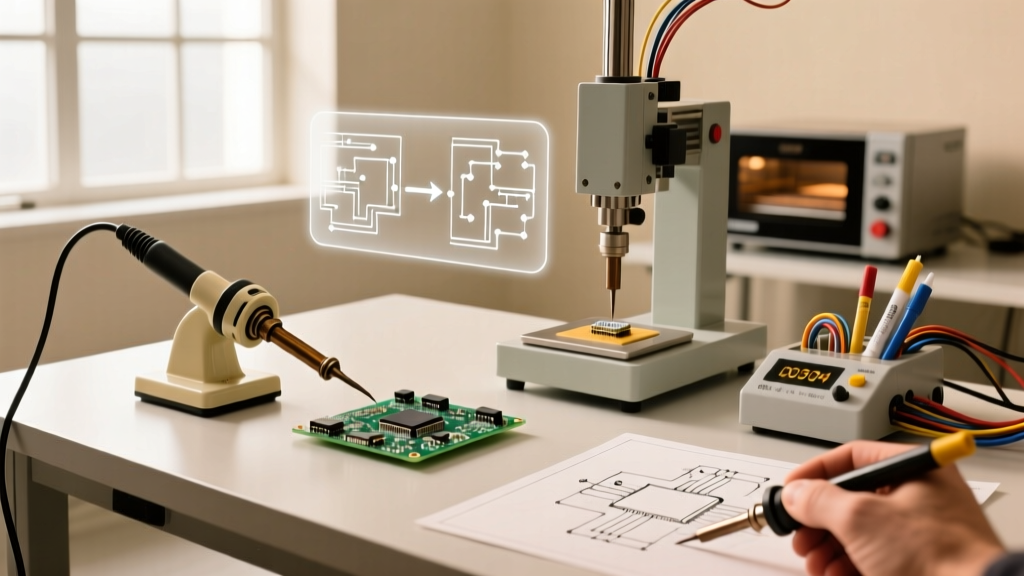

The Genesis: Point-to-Point and Early Phenolic Boards (1920s–1950s)
Before the concept of a printed circuit board (PCB) was fully realized, electronic assembly relied on point-to-point wiring. Components were mounted on turret terminals, tag boards, or early phenolic resin boards. During this era, soldering circuit board prototypes or radio chassis required massive, high-wattage copper irons—often exceeding 100W to 150W—to overcome the immense thermal mass of large metal chassis grounds and thick copper wires.
The solder alloy of choice was universally Sn60/Pb40 or the eutectic Sn63/Pb37, which melts at a predictable 183°C (361°F). Flux was primarily rosin-based (RMA), requiring manual cleaning with solvents like trichloroethylene. Because thermal profiles were entirely unregulated, early technicians relied on the 'spit test'—literally touching a wet finger to the iron—to gauge if it was hot enough to melt the lead-tin alloy without burning the rosin core.
The Through-Hole Era and the Wave Soldering Revolution (1960s–1980s)
The invention of the Plated Through-Hole (PTH) in the late 1950s revolutionized electronics. By electroplating copper through drilled holes in fiberglass-reinforced epoxy (FR-4) laminates, engineers could create multi-layer boards with reliable electrical connections between layers. However, hand-soldering hundreds of through-hole pins per board was economically unviable for mass production.
This bottleneck birthed the wave soldering machine. Pioneered by companies like Electrovert in the 1960s, wave soldering involved passing a populated PCB over a standing wave of molten Sn63/Pb37 solder at roughly 250°C. The board's bottom was first coated in a foaming liquid flux to prevent oxidation. While wave soldering dominated manufacturing, hand soldering remained the standard for rework and DIY. During this period, the first temperature-controlled irons, such as the iconic Weller TCP series utilizing Curie-point magnetic sensors, entered the market, preventing the catastrophic pad lift-off that plagued unregulated irons.
Surface Mount Technology (SMT) Changes the Paradigm (1980s–2000s)
As consumer electronics demanded smaller form factors, the industry shifted from Through-Hole Technology (THT) to Surface Mount Technology (SMT). Components were no longer inserted into holes; their leads were soldered directly onto surface pads. This fundamentally changed the physics of soldering circuit board assemblies. Instead of a high-thermal-mass iron melting a wire inside a barrel, technicians and machines now had to apply precise heat to flat, coplanar surfaces without damaging the delicate plastic bodies of Integrated Circuits (ICs).
SMT introduced solder paste—a thixotropic mixture of microscopic solder spheres and tacky flux—applied via laser-cut stainless steel stencils. Pick-and-place machines positioned components, and convection reflow ovens melted the paste using carefully calibrated thermal profiles (Preheat, Soak, Reflow, Cooling).
The RoHS Turning Point: In 2006, the European Union's Restriction of Hazardous Substances (RoHS) directive forced a global transition away from lead. The industry standard shifted to SAC305 (96.5% Tin, 3.0% Silver, 0.5% Copper). This raised the liquidus melting point from 183°C to 220°C, requiring peak reflow temperatures of 245°C. This 62°C increase caused widespread early-2000s failures, including PCB delamination and the notorious 'head-in-pillow' (HiP) BGA defects, forcing a total redesign of flux chemistries and thermal profiles (EU RoHS Directive).
The Modern Era: Micro-BGA, 008004 Components, and Laser Soldering (2010s–2026)
Today, the miniaturization of electronics has pushed the physical limits of metallurgy. Modern smartphones and IoT devices utilize 01005 (0.4mm x 0.2mm) and the bleeding-edge 008004 (0.25mm x 0.125mm) passive components. At this scale, a single human hair is thicker than the component itself. Soldering circuit board assemblies at this level requires Type 5 or Type 6 solder pastes (particle sizes under 15 microns) and advanced vapor-phase reflow ovens that use inert Galden fluids to guarantee oxygen-free, perfectly uniform heating.
For rework and repair, traditional hot air is often too turbulent, risking the displacement of adjacent micro-components. The modern rework station now incorporates laser soldering systems and localized micro-convection nozzles that target a single 0.2mm pad without raising the ambient temperature of the surrounding FR-4 substrate.
Component Miniaturization & Soldering Evolution Matrix
| Era | Dominant Package | Typical Dimensions | Primary Soldering Method | Key Failure Mode |
|---|---|---|---|---|
| 1960s-1970s | DIP (Dual In-line) | 7.62mm pitch | Wave / Hand Iron | Cold joints, bridging |
| 1980s-1990s | SOIC / QFP | 1.27mm - 0.5mm pitch | IR Reflow / Hot Air | Tombstoning, lead lift |
| 2000s-2010s | BGA / 0402 | 1.0mm ball / 1.0x0.5mm | Convection Reflow | Head-in-Pillow, voiding |
| 2020s-2026 | WLCSP / 008004 | 0.25x0.125mm | Vapor Phase / Laser | Pad cratering, thermal damage |
Translating History into Modern Workbench Purchases
Understanding this evolution is critical when buying equipment today. If you are repairing modern SMT boards, a vintage 60W Weller WES51 or a budget USB-C iron like the Pinecil V2 ($26) will fail you. While excellent for basic through-hole wiring or thick gauge XT60 connectors, they lack the thermal recovery and tip geometry required for modern lead-free SMT rework.
Here is how to align your tool purchases with the current state of PCB technology:
- For Advanced SMT Rework (BGA, QFN, 0201s): You need a high-thermal-capacity hot air station. The Quick 861DW (approx. $280) remains the industry benchmark for DIY and mid-level repair. Its 1200W heating element and 100L/min airflow allow you to reflow a 25x25mm BGA chip evenly without scorching the board. Pair this with a low-melt bismuth-based solder paste (melting at 138°C) to safely remove lead-free OEM components without exceeding the FR-4 glass transition temperature (Tg) of 170°C.
- For Precision Trace Repair and Micro-Soldering: Ditch traditional ceramic-heated irons. Invest in a cartridge-based system like the JBC CD-2BQE (approx. $550) using C245 handles. JBC's technology routes the heater directly to the tip's apex, achieving a 2-second thermal recovery. When dragging a 0.1mm micro-pencil tip across a 0.2mm trace to solder a microscopic jumper wire, the JBC maintains a stable 350°C, whereas traditional irons suffer a 40°C temperature drop upon contact with the copper pad.
- For Heavy Ground Planes (Through-Hole Legacy): If you are restoring vintage amplifiers or soldering thick 10AWG wires to battery tabs, thermal mass is your enemy. A high-wattage iron like the Hakko FX-951 (approx. $330) with a heavy chisel tip (T15-D52) or an induction-based Metcal system is required to prevent cold, crystalline solder joints caused by the ground plane acting as a massive heatsink.
Industry Standards and Reference Frameworks
Whether you are a hobbyist or a professional buyer, your soldering processes should align with modern reliability standards. The IPC J-STD-001 standard dictates the requirements for soldered electrical and electronic assemblies, defining acceptable wetting angles, fillet shapes, and voiding percentages for everything from Class 1 (general consumer electronics) to Class 3 (aerospace and medical life-support systems). When purchasing solder paste or flux, always verify that the chemical formulation meets IPC J-STD-004B standards for flux activity and corrosivity to ensure long-term reliability of your circuit boards.