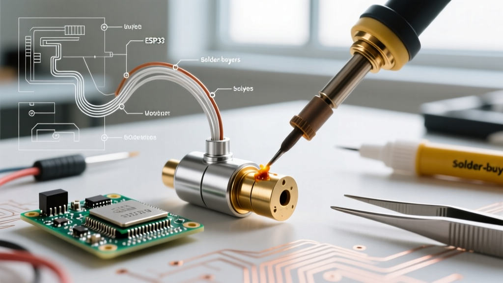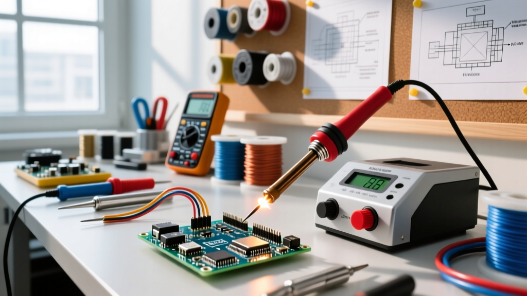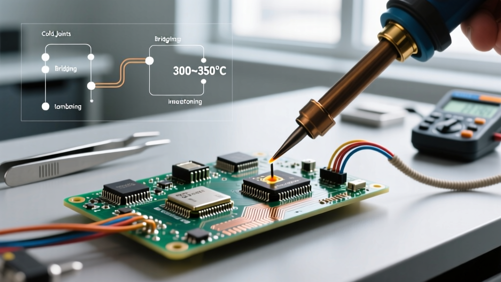

The True Definition of Soldering Defects (Soldering Def)
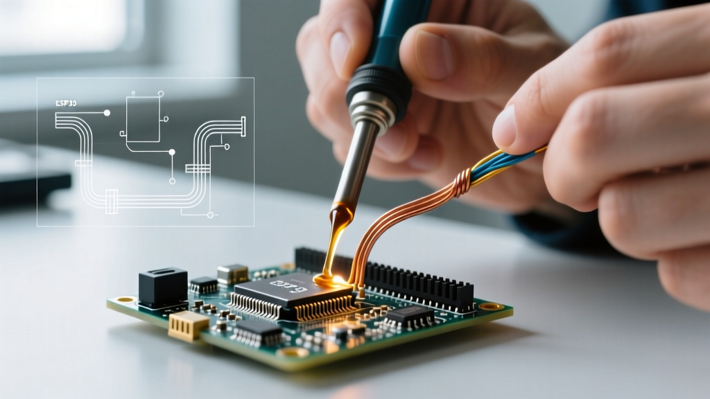
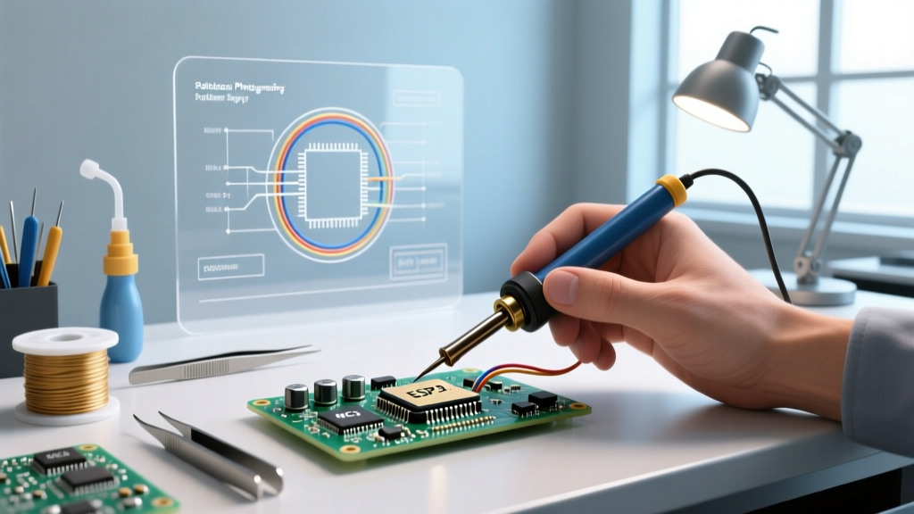
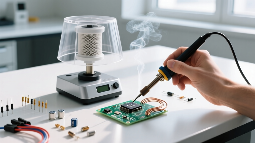
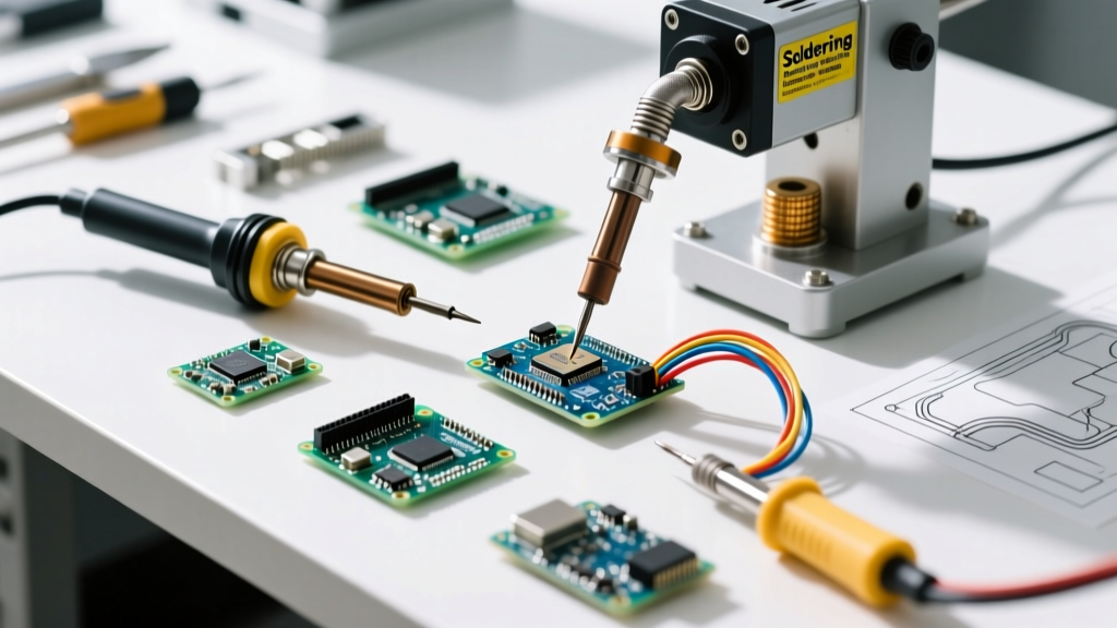
In the electronics manufacturing and DIY repair space, the abbreviation soldering def universally refers to soldering defects—anomalies in the solder joint that compromise electrical conductivity, mechanical strength, or long-term reliability. Whether you are hand-soldering a 0402 surface-mount resistor or assembling a high-power motor controller, understanding the exact definition and root cause of these defects is the difference between a lasting repair and a catastrophic field failure.
A perfect solder joint is not just about melting metal; it is a precise metallurgical process. When molten solder meets a copper pad, it forms an Intermetallic Compound (IMC) layer. According to materials science standards, an optimal IMC layer should be exactly 1 to 2 microns thick. If the iron is too cold, the IMC fails to form (resulting in a cold joint). If the dwell time exceeds 5 seconds, the IMC grows too thick, creating a brittle joint prone to micro-fractures under thermal cycling.
Grading Joints: The IPC-A-610 Standard
To objectively define what constitutes a defect, the industry relies on the IPC-A-610 Acceptability of Electronic Assemblies standard. This document categorizes solder joints into three distinct classes:
- Class 1 (General Electronic Products): Focuses on basic functionality. Minor cosmetic defects are acceptable if the joint is electrically sound.
- Class 2 (Dedicated Service Electronic Products): Requires extended life and uninterrupted performance. Most consumer electronics, automotive PCBs, and high-end DIY projects fall here.
- Class 3 (High-Performance Electronic Products): Zero tolerance for defects. Used in aerospace, medical life-support, and military hardware where failure is not an option.
Expert Insight: Many hobbyists aim for Class 1 but accidentally create Class 2 or 3 defects because they misunderstand thermal mass. Buying a $20 iron and pushing it to 400°C to compensate for poor thermal recovery is the fastest way to delaminate a PCB pad.
Top 4 Soldering Defects: Visuals, Causes, and Cures
1. Cold Solder Joints (The Grainy Menace)
Definition: A joint where the solder did not reach its liquidus temperature or the components moved during the cooling phase, preventing a proper IMC bond.
Visual Signs: The joint appears dull, grainy, gray, or bulbous rather than smooth and shiny (for leaded) or smoothly matte (for lead-free).
Root Cause: Insufficient heat transfer. For example, attempting to solder a thick ground plane with a 40W iron set to 280°C. The PCB acts as a massive heatsink, dropping the tip temperature below the melting point of SAC305 (217°C-220°C).
The Fix: Increase your iron's thermal capacity, not just its temperature. Apply high-quality tacky flux (like Amtech NC-559-V2-TF) and use a wider chisel tip (e.g., Hakko D24) to maximize surface area contact. Reheat the joint until the solder flows naturally, then remove the iron and hold the component perfectly still for 3-4 seconds.
2. Solder Bridges (Unintended Shorts)
Definition: An accidental electrical connection between two adjacent pads or pins caused by excess solder bridging the gap.
Visual Signs: A visible blob of solder connecting two distinct IC pins, often causing immediate short circuits or erratic microcontroller behavior.
Root Cause: Using too much solder wire, lacking adequate flux, or using a tip that is too large for the pitch of the component. Drag soldering a 0.5mm pitch QFP chip with a massive bevel tip guarantees bridges.
The Fix: Utilize the 'drag soldering' technique with a micro-chisel or fine conical tip. Apply copious amounts of no-clean liquid flux (such as MG Chemicals 8341) to the pads before applying heat. If a bridge occurs, do not panic; use a high-quality desoldering wick (Goot Wick or Chemtronics) with fresh flux to wick away the excess solder via capillary action.
3. Tombstoning (The SMD Nightmare)
Definition: A surface-mount defect where a passive component (like a capacitor or resistor) stands up on one end, resembling a tombstone.
Visual Signs: One pad is soldered, while the other end of the component is lifted vertically into the air.
Root Cause: Uneven heating. If one pad reaches reflow temperature before the other, the surface tension of the molten solder on the first pad will physically pull the component upright. This is highly common in 0402 and 0201 packages.
The Fix: Ensure both pads are heated simultaneously. If hand-soldering, pre-tin both pads equally, place the component with tweezers, and apply heat to the center of the component body or alternate rapidly between pads. For reflow ovens, ensure the PCB layout has balanced thermal relief on both pads to prevent uneven heat sinking.
4. Voids and Blowholes
Definition: Small pockets of gas trapped inside or beneath the solder joint.
Visual Signs: Pinholes on the surface of the solder fillet, or internal voids visible only via X-ray inspection.
Root Cause: Outgassing from low-quality flux, or moisture trapped inside the PCB substrate or component packaging (popcorning effect).
The Fix: Store moisture-sensitive components in dry cabinets or bake them at 125°C for 4 hours before soldering. Use a high-grade, low-voiding flux and ensure your soldering profile includes a proper preheat soak phase (ramping to 150°C over 90 seconds) to allow solvents to evaporate before the solder hits liquidus.
Buyer’s Matrix: Matching Gear to Defect Prevention
Preventing soldering defects requires matching your tool's thermal recovery rate to your workload. As of 2026, active-tip technology dominates the professional space, but high-end ceramic heaters remain viable for DIYers. Below is a buyer's matrix to help you select the right gear based on the defects you are trying to avoid.
| Primary Defect Risk | Required Tool Feature | Top 2026 Station Pick | Estimated Price Range |
|---|---|---|---|
| Cold Joints (Heavy Ground Planes) | High Wattage (150W+), Active Tip Tech, Fast Thermal Recovery | JBC CD-2BQE with C245 Tips | $550 - $650 |
| Solder Bridges (Fine Pitch SMD) | Precision Micro-Tips, ESD Safe, Low Voltage Tip-to-Ground | Hakko FX-951 with T18-J02 | $250 - $290 |
| Tombstoning (0402/0201 Passives) | Integrated Preheater + Fine Point Iron, Strict Temp Control | Weller WE1010NA + WPH800 Preheater | $220 - $260 |
| General DIY Defects (Through-Hole) | Portable, Smart Temp Profiling, USB-C PD Power | Pine64 Pinecil V2 | $26 - $35 |
Thermal Recovery: Why Cheap Irons Create Defects
Many beginners assume that setting a cheap $15 soldering iron to 450°C will melt solder faster. This is a fundamental misunderstanding of thermodynamics. A cheap iron may read 450°C on its dial, but the moment it touches a copper ground plane, its thermal mass plummets, and it cannot recover. The result? You hold the iron on the pad for 12 seconds, boiling the flux, oxidizing the tip, and creating a brittle, high-resistance cold joint.
Professional stations like the Hakko FX-951 or JBC C245 systems utilize active-tip technology where the heating element and temperature sensor are integrated directly inside the tip itself. This allows the station to detect a temperature drop in milliseconds and dump 70+ watts of power into the joint instantly. The solder flows in 1.5 seconds, the flux activates perfectly, and the IMC layer forms at the ideal 1-micron thickness. For comprehensive through-hole and basic SMD tutorials that emphasize these techniques, the SparkFun Soldering Guide remains an industry-standard reference.
Flux Chemistry: The Unsung Hero of Defect Prevention
You cannot buy your way out of soldering defects without understanding flux. Flux removes oxidation from the copper pads and the component leads, allowing the molten solder to 'wet' the surface. Without flux, solder will ball up and refuse to adhere, leading to severe bridging and cold joints.
- Rosin (RMA): Traditional, requires cleaning with isopropyl alcohol. Excellent for general electronics.
- No-Clean: Leaves a clear, non-conductive residue. Ideal for SMD work and dense PCBs where washing is impossible. (e.g., Kester 186).
- Water-Soluble: Highly active, great for heavily oxidized pads, but must be washed with distilled water immediately, or the acidic residue will corrode the traces over time.
For deeper insights into selecting the right chemistry for your specific PCB assembly, the Adafruit Guide to Excellent Soldering provides excellent visual breakdowns of flux behavior under heat.
FAQ: Troubleshooting Soldering Defs
Why does my soldering iron tip turn black and stop melting solder?
This is called tip oxidation, a defect caused by leaving the iron at high temperatures (above 380°C) without a protective layer of solder. To prevent this, always 'tin' your tip with a blob of cheap leaded solder before turning it off. If a tip is already black, use a brass wire tip cleaner (never sandpaper or a wet sponge, which causes thermal shock and micro-cracking) and apply fresh flux-cored solder to re-tin it.
Can I use lead-free solder for DIY repairs to avoid defects?
Lead-free solder (like SAC305) has a higher melting point (217°C) and poor wetting characteristics compared to leaded Sn63/Pb37 (183°C). For hand-soldering DIY repairs, leaded solder is vastly superior. It flows easier, requires less heat (reducing the risk of pad delamination), and produces naturally shiny joints, making visual defect inspection significantly easier.
How do I inspect for hidden soldering defects?
Visual inspection under a 10x to 45x stereo microscope is standard for Class 2 and Class 3 assemblies. For hidden defects like internal voids in BGA (Ball Grid Array) components, professional labs use X-ray inspection or thermal imaging cameras to detect high-resistance joints that generate excess heat under load.