
The Core Concept: What Defines an Arduino Schematic Maker?
In the microcontroller ecosystem, a schematic diagram maker is not merely a drawing tool; it is a logical database that bridges the gap between abstract circuit theory and physical printed circuit board (PCB) manufacturing. For Arduino makers, transitioning from a text-based IDE and physical breadboard to a dedicated electronic design automation (EDA) suite is the defining milestone between hobbyist prototyping and professional product development.
When evaluating a schematic diagram maker Arduino workflows demand, you are actually looking for three integrated modules: schematic capture (logical connections), footprint assignment (physical dimensions), and PCB layout (copper routing). While early maker culture relied heavily on 'breadboard view' software, the modern 2026 landscape requires tools that can handle high-speed signals, surface-mount device (SMD) miniaturization, and direct supply-chain integration.
The Breadboard vs. Schematic Paradigm Shift
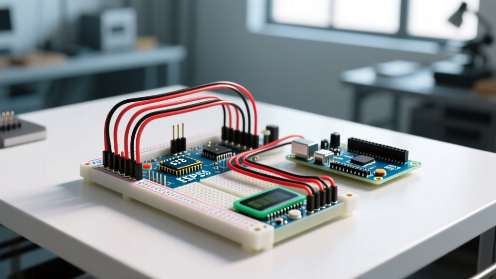
Physical breadboards obscure electrical reality. On a breadboard, a wire connecting Pin A to Pin B looks identical whether it is carrying a 5V power rail, a high-speed SPI clock signal, or a sensitive analog reference voltage. A proper schematic diagram maker strips away the physical illusion and forces the designer to think in terms of nets and nodes.
According to the official Arduino hardware documentation, understanding the logical netlist is critical for avoiding ground loops and signal interference. In a schematic, power distribution networks (PDNs) are explicitly defined, and decoupling capacitors are logically placed exactly where they are needed, rather than wherever there is physical space on a solderless board.
Tool Comparison Matrix: Fritzing vs. EasyEDA vs. KiCad
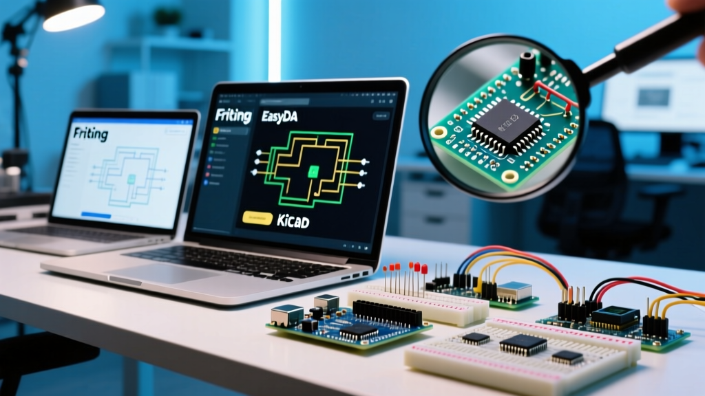
Choosing the right software depends on your end goal: quick visual documentation, rapid supply-chain prototyping, or professional-grade open-source design. Below is a technical comparison of the three dominant tools in the Arduino space.
| Feature | Fritzing | EasyEDA (Standard/Pro) | KiCad (v8+) |
|---|---|---|---|
| Primary Use Case | Beginner visual documentation | Rapid prototyping & JLCPCB integration | Professional open-source PCB design |
| Cost (2026) | $8.00 flat download fee | Free (Standard) / ~$99/yr (Pro) | 100% Free and Open Source |
| Learning Curve | Very Low (Drag-and-drop) | Moderate (Cloud-based UI) | High (Professional EDA paradigm) |
| Custom SMD Footprints | Poor (Manual SVG editing) | Excellent (LCSC linked library) | Excellent (Parametric footprint editor) |
| High-Speed Routing | Not supported | Basic (Pro version supports differential pairs) | Advanced (Push/shove, length tuning) |
| 3D PCB Preview | Basic (Static models) | Good (WebGL based) | Exceptional (Raytraced STEP export) |
Fritzing: The Visual Crutch and Its Limitations
Fritzing revolutionized maker documentation by introducing the 'breadboard view,' allowing users to create photorealistic diagrams of their Arduino Uno and jumper wire setups. However, as a true schematic diagram maker, it falls critically short for complex MCU designs. The software struggles with modern SMD components, and creating custom footprints requires tedious SVG manipulation. Furthermore, Fritzing's schematic view does not enforce electrical rules checking (ERC) rigorously, meaning you can easily wire a 5V logic pin directly to a 3.3V ESP32 input without the software flagging the fatal error.
Verdict: Use Fritzing strictly for creating beginner-friendly tutorial graphics. Do not use it for generating Gerber files for manufacturing.
EasyEDA: The Supply-Chain Integrated EDA
EasyEDA has become the default cloud-based schematic and PCB tool for makers who want to move from prototype to manufactured PCB in under 48 hours. Its killer feature is the deep integration with LCSC (a massive Asian electronic components distributor) and JLCPCB (a PCB fabrication house). When you place an ATmega328P-AU microcontroller in EasyEDA, you can simultaneously select the exact 100nF 0603 X7R decoupling capacitor (e.g., LCSC Part #C14663) and push the entire bill of materials (BOM) directly to the assembly line.
Verdict: The best choice for intermediate makers building custom Arduino shields, IoT sensor nodes, or standalone ESP32 boards where speed-to-market and component availability are paramount.
KiCad: The Professional Open-Source Standard
For engineers and advanced makers, KiCad is the undisputed champion. With the release of KiCad 8 and subsequent updates, the software features a modernized UI, an interactive push-and-shove router, and native support for differential pair tuning (essential for routing the USB D+/D- lines on native USB microcontrollers like the ATmega32U4 or SAMD21). KiCad's schematic editor enforces strict ERC, ensuring that power flags are properly managed and no pins are left floating.
Verdict: Mandatory for complex, multi-layer MCU designs, high-speed interfaces (SPI/QSPI flash), and projects intended for commercial open-source hardware release.
Real-World Failure Modes When Skipping Schematics
Makers who attempt to route a PCB directly from a breadboard mental model without drafting a proper schematic frequently encounter catastrophic hardware failures. Here are three specific edge cases that a robust schematic diagram maker prevents:
- The Decoupling Capacitor Distance Error: On a breadboard, a 100nF capacitor might sit two inches away from the MCU's VCC pin. In a PCB layout, if the schematic does not logically group the capacitor with the specific power pin, the router might place it across the board. This introduces parasitic inductance, rendering the capacitor useless at high frequencies and causing the MCU to brownout during PWM switching.
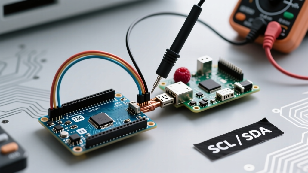
- Missing I2C Pull-Up Resistors: Breadboards often rely on the internal pull-ups of the Arduino Wire library, which are weak (20kΩ to 50kΩ). A proper schematic forces the designer to explicitly add 4.7kΩ external pull-up resistors to the SDA and SCL nets, ensuring reliable communication with sensors like the MPU6050 or BME280 at 400kHz Fast Mode.
- USB Impedance Mismatch: Designing a custom Arduino Leonardo (ATmega32U4) requires routing the USB data lines as a 90-ohm differential pair. Schematic tools like KiCad allow you to assign specific net classes to these pins, instructing the PCB router to maintain exact trace widths and spacing to prevent signal reflection and USB enumeration failures.
Step-by-Step: Migrating an Arduino Nano Clone to a Custom PCB
To illustrate the practical application of a schematic diagram maker, here is the exact workflow for migrating a breadboard Arduino Nano prototype into a standalone surface-mount PCB using EasyEDA or KiCad.
Step 1: Audit the Logical Connections
Ignore the physical colors of your jumper wires. Map out the nets: Which analog pins are reading sensors? Which digital pins are driving MOSFETs for high-current loads? Document the exact pinout of the ATmega328P, noting that the physical DIP-28 pin numbers on the Nano do not match the logical Arduino 'D' and 'A' designations.
Step 2: Draft the Schematic
Place the core MCU symbol. If you are moving from a through-hole DIP-28 to a surface-mount TQFP-32 (ATmega328P-AU), you must add the extra pins (ADC6, ADC7, and additional VCC/GND pairs) to your schematic that were internally unconnected on the DIP version. Add a 16MHz crystal oscillator with two 22pF load capacitors, and a 10kΩ pull-up resistor on the RESET line.
Step 3: Assign Footprints and Run ERC
Map every logical symbol to a physical footprint. Ensure your polarized components (electrolytic capacitors, diodes) have clear silkscreen markings. Run the Electrical Rules Check (ERC) to catch unconnected power pins or conflicting output drives.
Step 4: PCB Layout and Design Rule Check (DRC)
Import the netlist into the PCB editor. Set your design rules to a minimum trace width of 0.254mm (10 mil) for signal lines and 0.5mm (20 mil) for 5V/GND power rails. Place the decoupling capacitors within 2mm of the MCU VCC pins before routing any other traces. Use a ground pour on the bottom layer to provide a solid return path for high-frequency signals.
Step 5: Generate Manufacturing Files
Export the Gerber files (Extended Gerber RS-274X format) and the Excellon drill files. If using an assembly service, export the BOM and the Pick-and-Place (CPL) centroid file. Review the 3D viewer one last time to verify component clearances before submitting to the fabrication house.
Conclusion
Selecting the right schematic diagram maker for Arduino projects is about matching the tool to your engineering maturity. While Fritzing serves a niche in visual education, the modern maker must embrace the logical rigor of EasyEDA or KiCad. By treating your schematic as a mathematical blueprint rather than a simple drawing, you eliminate wiring ambiguities, optimize signal integrity, and unlock the true potential of custom microcontroller hardware design.