
The Hidden Time-Sink of SPI Wiring Workflows
In the embedded development lifecycle, few things drain momentum faster than a misconfigured Serial Peripheral Interface (SPI) bus. While I2C relies on addresses and UART on baud rates, SPI demands strict adherence to physical pinouts, clock phases, and voltage levels. When a maker or engineer transitions from a single-sensor prototype to a multi-device production workflow, guessing pinouts or relying on fragmented forum posts leads to hours of oscilloscope debugging.
Optimizing your SPI workflow isn't just about memorizing which pin is MOSI; it is about establishing a systematic approach to hardware routing, Chip Select (CS) management, and logic-level translation. This guide provides a deep-dive framework for mastering the SPI pinout across modern microcontrollers, eliminating physical layer bottlenecks, and accelerating your path from breadboard to PCB.
Deconstructing the Pinout: The Shift to CIPO/COPI
For decades, the standard SPI pinout relied on the MOSI (Master Out Slave In) and MISO (Master In Slave Out) nomenclature. However, modern engineering workflows are actively shifting toward more inclusive and functionally accurate terminology: COPI (Controller Out Peripheral In) and CIPO (Controller In Peripheral Out).
The Open Source Hardware Association (OSHW) officially recommended the CIPO/COPI naming convention to eliminate ambiguous master/slave terminology while better describing the data flow direction relative to the controller (OSHW Resolution).
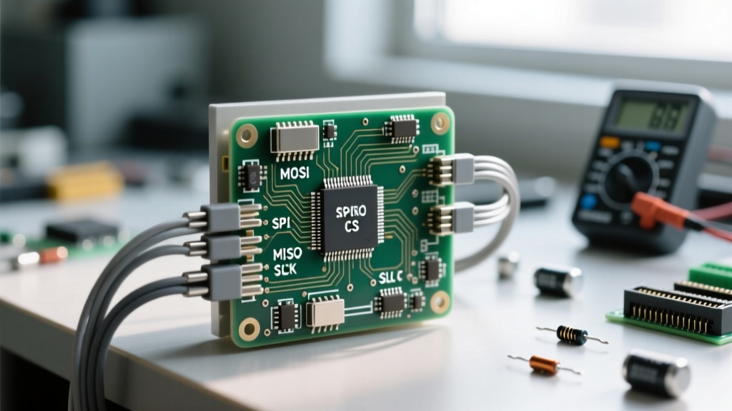
When mapping your physical SPI pinout, the core four wires remain functionally identical:
- SCK (Serial Clock): The heartbeat generated by the controller.
- COPI (formerly MOSI): Data line from Controller to Peripheral.
- CIPO (formerly MISO): Data line from Peripheral to Controller.
- CS/SS (Chip Select/Slave Select): Active-low trigger for individual peripherals.
Cross-MCU Hardware SPI Pinout Matrix
A major workflow bottleneck occurs when migrating code between MCU families. Software SPI (bit-banging) is flexible but CPU-intensive. Hardware SPI requires exact pin mapping. Below is a reference matrix for the most common development boards used in 2026 maker workflows.
| MCU / Board | SPI Bus | SCK | COPI (MOSI) | CIPO (MISO) | Default CS |
|---|---|---|---|---|---|
| Arduino Uno R3 (ATmega328P) | SPI | 13 | 11 | 12 | 10 |
| ESP32 DevKit V1 | VSPI | 18 | 23 | 19 | 5 |
| ESP32 DevKit V1 | HSPI | 14 | 13 | 12 | 15 |
| Raspberry Pi Pico (RP2040) | SPI0 | 18 | 19 | 16 | 17 |
| STM32F103C8T6 (Blue Pill) | SPI1 | PA5 | PA7 | PA6 | PA4 |
Workflow Tip: On the ESP32, the Espressif SPI Master API allows you to remap VSPI and HSPI pins via the GPIO matrix, but sticking to the default hardware routes minimizes parasitic routing delays and simplifies PCB layout.
Workflow Optimization 1: Escaping the Breadboard Parasitic Trap
When prototyping high-speed SPI devices (like TFT displays or external ADCs sampling at >5 MSPS), the physical environment of your pinout matters as much as the logical mapping. Standard 400-point solderless breadboards introduce roughly 2pF to 5pF of parasitic capacitance per contact strip.
At SPI clock speeds exceeding 8 MHz, this capacitance forms a low-pass filter with the output impedance of your MCU's GPIO pins. The result? Square clock waves degrade into shark-fin shapes, causing the peripheral to misread the SCK rising edges.
The Twisted-Pair Protocol
To optimize your physical wiring workflow without jumping straight to a PCB:
- Use short, 22AWG solid-core wires for SCK and CS.
- Twist the COPI and CIPO lines together with a common ground wire to minimize inductive crosstalk.
- Never route SCK parallel to high-current PWM lines (like motor driver outputs).
Workflow Optimization 2: The Chip Select (CS) Bottleneck
The standard SPI pinout shares SCK, COPI, and CIPO across all devices, but requires a dedicated CS pin for every single peripheral. If your project integrates an SD card, an IMU, and a thermocouple amplifier, you have instantly consumed three valuable GPIOs just for routing.
Multiplexing vs. Daisy Chaining
Rather than burning through your MCU's pinout, optimize your workflow using a 74HC138 3-to-8 line decoder. By wiring three MCU GPIOs to the 74HC138's select pins, you can independently trigger up to eight SPI Chip Select lines. This drastically simplifies the physical harness, reduces wire clutter, and frees up the MCU's pinout for analog inputs or interrupt handlers.
Alternatively, if your SPI peripherals support it (like the MAX31855 or MAX7219), utilize the daisy-chain (CIPO-to-COPI) topology. This allows you to string multiple ICs together using a single CS pin, shifting data through the chain like a shift register.
The Level Shifter Trap: Why Auto-Sensing ICs Fail at 10MHz
Mixing 5V (Arduino Uno) and 3.3V (ESP32/RP2040) logic on the same SPI bus is a rite of passage. Many makers default to the TXB0108 bidirectional auto-sensing level shifter because it requires no direction pin. This is a critical workflow error for high-speed SPI.
The TXB0108 utilizes internal one-shot edge-rate boosters and relies on low capacitive loads. The inherent capacitance of an SPI CIPO line, combined with breadboard wiring, often causes the TXB0108 to enter a high-frequency oscillation state, completely corrupting the SPI pinout data.
The Correct Translation Workflow
- For 3.3V to 5V (Controller to Peripheral): Use a CD4050 non-inverting buffer. It is cheap, handles high capacitance, and easily passes 20MHz SPI clocks.
- For 5V to 3.3V (Peripheral to Controller): Use a 74LVC125 or a simple BSS138 MOSFET bidirectional circuit, ensuring pull-up resistors are kept to 2.2kΩ or lower to maintain sharp rising edges.
- Dedicated SPI Shifters: The 74AHCT125 is the gold standard for directional SPI level translation, providing clean edges without the oscillation risks of auto-sensing ICs.
Systematic Triage: When the Pinout is Correct but the Bus is Dead
Even with a perfect physical SPI pinout, communication often fails. Before rewriting your Arduino SPI library code, execute this 3-step hardware triage using a logic analyzer (a $60 DSLogic Plus is sufficient for most maker workflows).
Step 1: Verify CPOL and CPHA (SPI Modes)
SPI defines four modes based on Clock Polarity (CPOL) and Clock Phase (CPHA). If your peripheral expects Mode 3 (Clock idle HIGH, data sampled on falling edge) and your MCU defaults to Mode 0 (Clock idle LOW, sampled on rising edge), the data will be garbage. Always initialize your bus explicitly: SPISettings(10000000, MSBFIRST, SPI_MODE0).
Step 2: Check the Chip Select Timing
Some ADCs and sensors require a minimum 'CS setup time' (often 50ns to 100ns) before the first SCK pulse. If your MCU is clocking data out immediately after pulling CS LOW, the peripheral will ignore the transaction. Insert a microsecond delay or rely on hardware SPI peripherals that handle CS assertion automatically.
Step 3: Inspect for Ground Bounce
If your logic analyzer shows clean SCK pulses but the CIPO line is erratic, check your ground returns. High-speed SPI toggling draws fast transient currents. If the MCU and peripheral share a thin, high-inductance ground wire, 'ground bounce' will shift the logic threshold, causing the receiver to misinterpret 1s and 0s. Always use a star-ground topology or a solid ground plane in your physical layout.
Conclusion: Standardize to Accelerate
Mastering the SPI pinout is less about memorization and more about establishing robust engineering habits. By adopting the CIPO/COPI nomenclature, respecting parasitic capacitance in physical layouts, intelligently multiplexing CS lines, and avoiding auto-sensing level shifters on high-speed buses, you transform SPI from a frustrating debugging exercise into a reliable, high-throughput data pipeline. Standardize your hardware triage workflow today, and your future self will thank you when the next prototype boots up flawlessly on the first try.