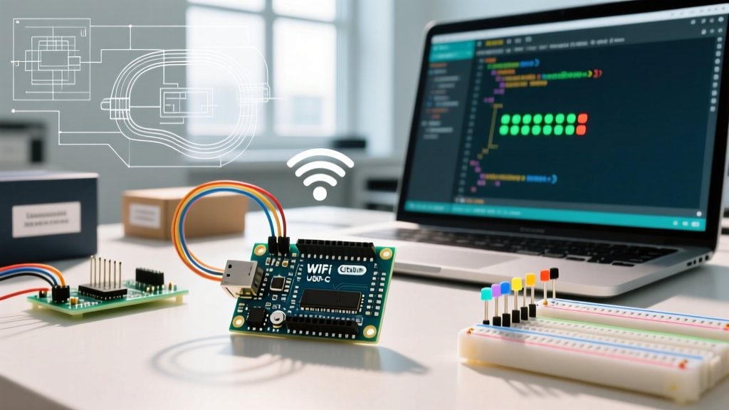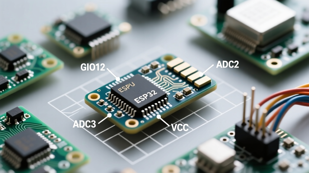

The Anatomy of an ESP32 Pinout Diagram
When transitioning from 8-bit AVR microcontrollers to the dual-core powerhouse that is the ESP32, the first hurdle every maker and hardware engineer faces is deciphering the ESP32 pinout diagram. Unlike the straightforward, almost foolproof pinouts of the Arduino Uno, the ESP32 (specifically the ubiquitous ESP32-WROOM-32 module) is a highly multiplexed system-on-chip (SoC). Almost every General Purpose Input/Output (GPIO) pin shares multiple peripheral functions, from UART and SPI to capacitive touch and analog-to-digital conversion.
However, not all pins are created equal. A standard ESP32 pinout diagram might show 30 to 38 exposed pins depending on your DevKit (such as the NodeMCU-32S or the DOIT ESP32 DEVKIT V1), but treating them as interchangeable is a fast track to boot loops, fried silicon, and erratic sensor readings. This compatibility guide cuts through the marketing fluff to provide a strict, real-world engineering framework for selecting the right pins for your next IoT or robotics project.
The 'Input-Only' Trap: GPIOs 34 through 39
One of the most common hardware design errors among beginners is attempting to drive a relay, LED, or logic gate using the high-numbered GPIOs. According to the official Espressif ESP32 Datasheet, GPIOs 34, 35, 36 (VP), and 39 (VN) are strictly input-only pins.
Furthermore, these pins lack internal pull-up and pull-down resistors. If you are wiring a simple push-button or a digital sensor to these pins, you must provide external pull-up or pull-down resistors (typically 10kΩ) to prevent the pin from floating. Interestingly, GPIO 36 and 39 are also tied to the chip's internal ultra-low-noise preamplifier and hall effect sensor, making them highly susceptible to electromagnetic interference (EMI) if routed near high-current traces on a custom PCB.
Critical Boot Strapping Pins: What You Must Avoid
The ESP32 relies on specific 'strapping pins' to determine its boot mode and flash voltage configuration during power-on or reset. If these pins are held at the wrong logic level by external sensors or pull-down resistors, the chip will fail to boot, often manifesting as a continuous serial monitor reset loop.
- GPIO 0: Determines boot mode. Must be HIGH for normal SPI flash boot, or LOW to enter the serial bootloader. Avoid connecting external pull-downs here.
- GPIO 2: Also tied to boot mode. Must be LOW or floating to boot from the internal SPI flash. Connecting an LED with a pull-up to this pin will brick the boot sequence.
- GPIO 12 (MTDI): Dictates the flash voltage. If pulled HIGH during boot, the ESP32 expects a 1.8V SPI flash chip. Since 99% of DevKits use 3.3V flash, pulling GPIO 12 HIGH will cause a fatal brownout and boot failure.
- GPIO 15 (MTDO): Controls boot log output and SDIO timing. Generally safer, but best left unburdened during the boot sequence.
Expert PCB Design Tip: If your schematic requires the use of GPIO 0 or GPIO 2 for a peripheral, ensure the peripheral defaults to a HIGH impedance state on power-up, or use a jumper/switch that only engages after the ESP32 has passed the bootloader phase.
The ADC2 and Wi-Fi Conflict Matrix
The ESP32 features two Analog-to-Digital Converters: ADC1 and ADC2. A critical compatibility constraint that catches many developers off guard is the mutual exclusivity of ADC2 and the Wi-Fi radio. The Wi-Fi subsystem requires exclusive access to the ADC2 hardware interrupt channels. If your sketch initializes WiFi.begin(), any attempt to read from an ADC2 pin using analogRead() will silently fail or return garbage data.
Below is the definitive compatibility matrix for mapping your analog sensors:
| ADC Channel | Associated GPIO Pins | Wi-Fi Compatibility | Bluetooth Compatibility | Recommended Use Case |
|---|---|---|---|---|
| ADC1 | 32, 33, 34, 35, 36, 39 | ✅ Fully Compatible | ✅ Fully Compatible | Battery monitoring, environmental sensors, potentiometers |
| ADC2 | 0, 2, 4, 12, 13, 14, 15, 25, 26, 27 | ❌ Conflicts (Fails) | ✅ Compatible | Offline data logging, BLE-only beacon projects |
Source: ESP-IDF ADC API Reference
5V Tolerance and Level Shifting Realities
Let's address a persistent myth found on older forums: The ESP32 is NOT 5V tolerant. The silicon operates strictly at 3.3V logic levels. While the 'VIN' or '5V' pin on a development board is simply a pass-through from the USB power rail (useful for powering 5V sensors like the HC-SR04 ultrasonic module), feeding a 5V logic signal directly into an ESP32 GPIO pin will degrade the internal ESD protection diodes and eventually destroy the SoC.
When integrating 5V legacy Arduino shields or industrial 5V PLCs, you must implement logic level shifting. For high-speed buses like SPI or I2C, a bidirectional MOSFET-based level shifter (like the BSS138 breakout boards) is mandatory. For unidirectional signals (e.g., reading a 5V rotary encoder), a simple CD4050 non-inverting buffer powered at 3.3V will safely clamp the logic levels.
Deep Sleep and RTC GPIO Compatibility
Power efficiency is a primary reason engineers choose the ESP32. However, waking the chip from Deep Sleep requires specific hardware routing. Standard GPIOs lose their state and power during deep sleep. To wake the ESP32 via an external interrupt (like a PIR motion sensor or a reed switch), you must use the RTC (Real-Time Clock) GPIOs.
The RTC domain includes GPIOs 0, 2, 4, 12, 13, 14, 15, 25, 26, 27, 32, 33, 34, 35, 36, and 39. When designing a battery-powered node, map your wake-up sources exclusively to these pins and utilize the esp_sleep_enable_ext0_wakeup() or ext1 APIs in your Arduino sketch. Attempting to wake the chip using a non-RTC GPIO like GPIO 16 will result in the chip sleeping indefinitely until a manual hardware reset.
Design Framework: Selecting Pins for Your Next PCB
To synthesize this data into an actionable workflow, follow this hierarchical pin-selection framework when drafting your schematic in KiCad or Altium:
- Allocate Communication Buses First: Reserve the default hardware I2C pins (GPIO 21 for SDA, GPIO 22 for SCL) and default SPI pins (GPIO 18, 19, 23) to ensure maximum compatibility with standard Arduino libraries.
- Assign Safe Analog Inputs: Map all analog sensors to ADC1 (GPIO 32, 33) to guarantee uninterrupted operation alongside Wi-Fi telemetry.
- Map Actuators and Outputs: Assign relays, motor drivers, and LEDs to the 'Safe Zone' GPIOs (16, 17, 18, 19, 21, 22, 23, 25, 26, 27, 32, 33). These pins have no boot-strapping conflicts and feature robust internal pull-up/down capabilities.
- Isolate Strapping and TX/RX Pins: Keep GPIO 1 (TX), 3 (RX), 0, 2, 12, and 15 completely isolated from external circuitry that might force a logic state during the first 800ms of power-on.
By treating the ESP32 pinout diagram not just as a map, but as a strict set of hardware constraints, you eliminate the most common integration failures. For a visual reference and interactive tool to verify your specific board variant, the community-maintained ESP32 Pinout Reference by Random Nerd Tutorials remains an invaluable bookmark for the workbench.