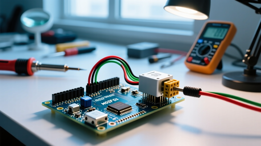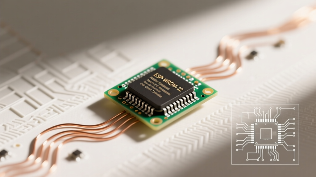

The ESP-WROOM-32 is a surface-mount Wi-Fi and Bluetooth module that packages the ESP32 system-on-chip, 4MB SPI flash memory, and a PCB trace antenna into a single metal-shielded footprint for custom PCB integration. Swapping a breadboard-friendly development kit for this bare module changes your design from a plug-and-play hobby project into a compact, production-ready embedded system that demands strict RF keepout zones and precise 3.3V power delivery. Makers and junior engineers constantly confuse the bare module with the underlying silicon chip or the carrier development board, leading to severe layout errors, incorrect schematic footprints, and sourcing mistakes.
The Silicon vs. The Module vs. The Dev Board
To design with this hardware, you must separate the terminology. The ecosystem is built in three distinct layers, and confusing them will result in ordering the wrong components or designing an unmanufacturable PCB.
- The ESP32 (The Silicon): This is the bare system-on-chip (SoC), such as the ESP32-D0WDQ6. It is a tiny QFN package that requires you to design external RF matching networks, route high-speed SPI lines to an external flash chip, and design your own antenna or U.FL connector circuit. Unless you are manufacturing 100,000+ units, you rarely use the bare silicon.
- The ESP-WROOM-32 (The Module): This is the metal-can surface-mount component. It integrates the bare SoC, a 40MHz crystal, 4MB of SPI flash, and the RF matching network onto a tiny internal PCB, all covered by an EMI shield. It exposes castellated pads for your main board to solder to.
- The ESP32 DevKit (The Carrier Board): This is the breadboard-friendly PCB that hosts the WROOM module alongside a USB-to-UART bridge (like a CP2102 or CH340), a 5V-to-3.3V voltage regulator, and an auto-reset circuit for flashing firmware.
Power Delivery and Thermal Limits: A Numeric Example
The most common point of failure when moving from a DevKit to a bare ESP-WROOM-32 on a custom board is the power supply. The ESP32 is notorious for aggressive current spikes during Wi-Fi transmission.
According to the official Espressif ESP32 Datasheet, the peak TX current is roughly 240mA during 802.11n transmission. Let us calculate the thermal reality of powering this module from a 5V USB rail using a standard SOT-223 linear dropout regulator (LDO) like the AMS1117-3.3.
- Voltage Drop: 5.0V (Input) - 3.3V (Output) = 1.7V drop across the LDO.
- Power Dissipated at Peak: P = V × I = 1.7V × 0.240A = 0.408 Watts.
- Thermal Resistance: A standard SOT-223 package on a 2-layer FR4 PCB has a junction-to-ambient thermal resistance ($\theta_{JA}$) of roughly 100°C/W.
- Temperature Rise: 0.408W × 100°C/W = 40.8°C rise.
- Final Junction Temp: 25°C (Ambient) + 40.8°C = 65.8°C.
At 65.8°C, the LDO survives, but it will be hot to the touch. However, if your custom board also includes a 5V relay or a high-draw sensor that pushes the continuous load to 400mA, the LDO will exceed its 125°C thermal shutdown threshold and reboot your ESP32 continuously.
The Fix: For mains-powered custom boards, use a switching buck converter (like the AP63203) which operates at >85% efficiency and barely warms up. For battery-powered IoT nodes, the AMS1117 is entirely unsuitable due to its ~5mA quiescent current, which will drain a 2000mAh 18650 cell in less than a month even in deep sleep. Use a low-IQ LDO like the MCP1700 or RT9013 instead.
Where You Meet the ESP-WROOM-32 in Practice
You will encounter this specific module when transitioning a prototype into a commercial or semi-commercial product. The primary advantage of the WROOM series is modular FCC/CE pre-certification. Because Espressif has already passed the expensive radiated emissions testing for the metal-shielded module, you inherit their certification—saving $10,000 to $15,000 in lab fees—provided you follow their integration rules.
The most critical integration rule is the RF keepout zone. The ESP-WROOM-32 uses a PCB trace antenna etched onto the module itself. The Espressif Hardware Design Guidelines mandate a strict keepout area on your host PCB. You must remove all copper pours, ground planes, signal traces, and vias from the top, bottom, and inner layers directly beneath and in front of the antenna overhang. Think of this keepout zone as an invisible electromagnetic forcefield; if your ground plane creeps into this 10mm × 15mm void, it will capacitively detune the antenna, dropping your practical Wi-Fi range from 50 meters down to 2 meters.
The 2026 Standard: Migrating to the ESP-WROOM-32E
If you are starting a new schematic today, you should default to the ESP-WROOM-32E rather than the original non-E variant. While pin-compatible for most layouts, the 'E' variant includes a 40MHz SPI flash (up from 26MHz), which significantly improves execute-in-place (XIP) performance for heavy codebases. More importantly for battery designers, the 'E' variant features refined deep-sleep architecture, reducing leakage currents and making Coulomb counting and battery life predictions far more accurate in low-power field deployments.
ESP-WROOM-32 Frequently Asked Questions
Can I use the bare ESP-WROOM-32 on a standard solderless breadboard?
No. The castellated pads on the ESP-WROOM-32 have a pitch of 0.9mm, which is entirely incompatible with standard 2.54mm (0.1-inch) solderless breadboards. To prototype with the bare module, you must solder it to a 0.9mm-to-2.54mm pitch adapter breakout board, or simply use an ESP32 DevKit which has already broken these pins out to standard headers.
What is the exact physical keepout zone for the ESP-WROOM-32 antenna?
You must maintain a minimum clearance void of 10mm × 15mm directly under the module's antenna overhang and extending outward. This area must be completely free of copper, traces, components, and vios on every layer of your host PCB. Additionally, keep the module at least 5mm away from the edge of your PCB enclosure if the enclosure contains any conductive materials or metallic paints.
Why does my ESP-WROOM-32 brownout when transmitting over Wi-Fi?
This is almost always caused by voltage droop during the 240mA transmission spike. If your 3.3V power trace is too long or too thin, the trace resistance causes a voltage drop ($V = I \times R$). If the voltage at the module's VDD33 pin dips below 2.2V even for a microsecond, the internal brownout detector (BOD) triggers and resets the chip. To fix this, widen your 3.3V power traces to at least 20mil and place a 10µF to 22µF X7R ceramic bulk capacitor as physically close to the module's VDD33 and GND pads as possible.
Do I need to design my own RF matching network for this module?
No. The ESP-WROOM-32 integrates the Pi-type RF impedance matching network internally. Your only job on the host PCB is to route a 50-ohm controlled impedance microstrip trace from the module's ANT pad to your U.FL connector or external chip antenna. Do not place any vias on this RF trace, and keep it as short and straight as possible, flanked by a ground plane on the same layer with adequate clearance to maintain the 50-ohm geometry.