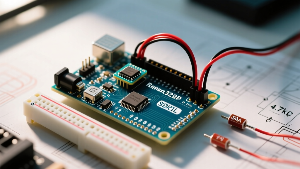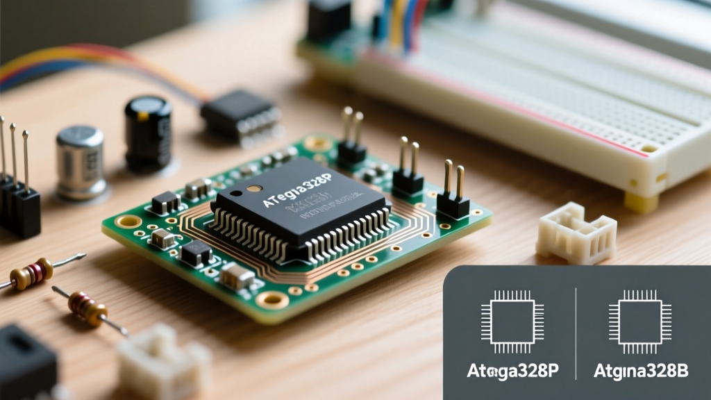

The Arduino Uno revolutionized maker electronics, cementing the AVR ATmega328P as the undisputed industry standard for 8-bit prototyping. However, as projects scale toward IoT connectivity, high-speed data acquisition, or complex motor control, engineers inevitably face the need to migrate. Whether you are dealing with silicon supply chain bottlenecks or simply outgrowing 2KB of SRAM, understanding the foundational atmega 328p pinout is critical for planning a seamless hardware upgrade.
This guide moves beyond basic hobbyist tutorials. We will deconstruct the legacy I/O architecture, evaluate drop-in AVR replacements like the ATmega328PB and LGT8F328P, and provide a rigorous framework for mapping legacy 5V pins to modern 3.3V 32-bit ecosystems like the ESP32 and STM32.
Deconstructing the Legacy Baseline Architecture
When engineers search for the atmega 328p pinout, they are usually referencing the standard 28-pin PDIP layout popularized by the Arduino Uno and countless custom PCBs. To plan a migration, you must understand how these 28 pins are grouped into logical ports, as this dictates how your firmware interacts with the silicon via registers like DDRB, PORTC, and PIND.
- Port B (PB0-PB7): Handles the SPI bus (MOSI, MISO, SCK) and the crystal oscillator pins (XTAL1, XTAL2). PB6 and PB7 double as PCINT (Pin Change Interrupt) sources, crucial for rotary encoder decoding.
- Port C (PC0-PC5): The analog domain. PC0-PC5 map to ADC0-ADC5. PC4 and PC5 also serve as the hardware TWI (I2C) bus (SDA/SCL). PC6 is permanently dedicated as the active-low RESET pin.
- Port D (PD0-PD7): The high-speed digital and communication hub. PD0/PD1 handle hardware UART (RX/TX). PD2 and PD3 are the dedicated hardware external interrupts (INT0 and INT1), essential for precise timing applications.
- Power & Analog Reference: VCC, GND, AVCC, and AREF. A common failure mode in custom PCB migrations is neglecting AVCC. Even if you do not use the ADC, AVCC must be tied to VCC (preferably through a ferrite bead) with a 100nF decoupling capacitor, or the chip will exhibit erratic digital behavior.
Drop-In Upgrades: ATmega328PB vs. LGT8F328P
If your project requires more I/O or processing headroom but you want to retain the 8-bit AVR instruction set and existing C/C++ codebase, drop-in upgrades are the logical next step. However, 'drop-in' is a relative term when examining the physical pinout.
| Feature | ATmega328P (PDIP-28) | ATmega328PB (TQFP-48) | LGT8F328P (TQFP-32) |
|---|---|---|---|
| Max Clock Speed | 20 MHz | 20 MHz | 32 MHz |
| Flash / SRAM | 32KB / 2KB | 32KB / 2KB | 32KB / 2KB |
| I2C / SPI / UART | 1 / 1 / 1 | 2 / 2 / 2 | 1 / 1 / 1 |
| ADC Resolution | 10-bit | 10-bit | 12-bit |
| DAC Output | None | None | 1x 8-bit DAC |
| Package Pins | 28 | 48 | 32 |
The ATmega328PB Migration Reality
According to the Microchip official product documentation, the ATmega328PB is fully backward compatible with the 328P in software. However, the hardware pinout tells a different story. To expose the second I2C bus, second SPI bus, and Port E, Microchip utilized a 48-pin TQFP package. If your legacy PCB uses a 28-pin DIP socket or a 32-pin TQFP footprint, the 328PB will not physically fit without a custom interposer board.
The Logic Green LGT8F328P Alternative
The LGT8F328P is a third-party AVR-compatible clone that runs natively at 32MHz and includes a 12-bit ADC and an internal 8-bit DAC. In the TQFP-32 package, the first 28 pins map almost identically to the standard 328P, making it an excellent upgrade path for existing SMD PCBs. The DAC is exposed on pin 32 (PE0), allowing for analog output generation without external PWM filtering. Be aware that migrating to the LGT8F328P requires installing the Logic Green board support package (BSP) in your IDE, as the internal oscillator and ADC registers differ slightly from the genuine Microchip silicon.
Migrating to 32-Bit: Mapping Legacy I/O to ESP32 and STM32
When 8-bit architectures hit a hard wall—whether due to the need for native Wi-Fi, Bluetooth, or 32-bit floating-point math—engineers must migrate to 32-bit MCUs. The challenge is mapping the mental model of the Arduino/328P pinout to entirely different silicon architectures.
Mapping the I2C and SPI Buses
On the 328P, hardware I2C is locked to PC4 (SDA) and PC5 (SCL). When migrating to the ESP32-WROOM-32, the I2C peripheral can be mapped to almost any GPIO via the GPIO matrix, but the Arduino core defaults to GPIO 21 (SDA) and GPIO 22 (SCL). Similarly, the 328P SPI bus (PB3, PB4, PB5) maps to the ESP32's default VSPI pins: GPIO 23 (MOSI), GPIO 19 (MISO), and GPIO 18 (SCK).
Expert Migration Tip: Never rely on internal pull-up resistors when migrating I2C buses from a 5V ATmega328P to a 3.3V ESP32. The internal pull-ups are typically 40kΩ to 50kΩ, which is far too weak for high-speed I2C. Always use external 4.7kΩ or 2.2kΩ resistors tied to the 3.3V VCC rail on the new MCU.
The 5V to 3.3V Logic Level Danger Zone
The most catastrophic failure mode during migration is ignoring logic level thresholds. The ATmega328P operates at 5V, meaning a HIGH signal outputs ~4.8V. The ESP32 and STM32F103 operate at 3.3V. Feeding a 5V signal directly into an ESP32 GPIO will forward-bias the internal ESD protection diodes. This causes 'phantom power' to backfeed into the 3.3V rail, leading to silicon degradation, erratic Wi-Fi resets, or immediate thermal latch-up. You must integrate a bidirectional logic level shifter (like the TXS0108E) or a discrete BSS138 MOSFET circuit on all migrating digital lines.
Interrupt and Timer Migration Realities
Firmware migration is often harder than hardware migration. On the ATmega328P, hardware external interrupts are scarce: only PD2 (INT0) and PD3 (INT1) support dedicated hardware interrupt vectors. Pin Change Interrupts (PCINT) are available on all Port B and Port D pins, but they share interrupt vectors, requiring software polling to determine which pin triggered the event.
When migrating to an STM32F103C8T6 (the popular 'Blue Pill'), the architecture shifts dramatically. According to the STMicroelectronics STM32F103 reference documentation, almost every GPIO pin can trigger a hardware interrupt via the EXTI controller. However, the EXTI lines are shared across ports. For example, PA0 and PB0 both map to EXTI Line 0. You cannot attach separate interrupt handlers to PA0 and PB0 simultaneously. Engineers migrating legacy 328P code must completely refactor their interrupt service routines (ISRs) to account for the STM32's NVIC (Nested Vectored Interrupt Controller) priority system.
PCB Layout Rules for Upgraded MCUs
If you are redesigning your PCB to accommodate a migrated MCU, specific layout rules must be followed to ensure signal integrity, especially when moving away from the forgiving PDIP-28 socketed form factor.
- Decoupling Strategy: The 328P requires a 100nF X7R ceramic capacitor placed as close to the VCC and AVCC pins as possible. When migrating to the 328PB (TQFP-48) or STM32, which feature multiple VCC/VDD pins, every single power pin requires its own dedicated 100nF capacitor. Sharing a single capacitor across multiple VDD pins will result in high-frequency noise coupling and ADC inaccuracy.
- Crystal Routing: If your migration retains an external crystal oscillator, keep the traces from the XTAL pins to the crystal under 15mm. Use 22pF C0G/NP0 load capacitors (avoid X7R/Y5V dielectrics due to their voltage and temperature coefficients). Route a ground moat underneath the crystal to prevent digital switching noise from coupling into the oscillator.
- The RESET Pin Pull-Up: The ATmega328P requires a 10kΩ pull-up resistor on the PC6/RESET pin. In noisy industrial environments, migrating to a new PCB without this pull-up will result in spontaneous resets caused by EMI spikes. Furthermore, if migrating to an ESP32, the EN (Enable) pin serves as the reset and requires a similar 10kΩ pull-up to VCC, alongside a 1uF capacitor to ground to prevent brown-out spikes during boot.
Strategic Summary for Hardware Engineers
Migrating away from the classic AVR ecosystem is a rite of passage for embedded systems engineers. By deeply understanding the baseline atmega 328p pinout, you can accurately audit your legacy I/O requirements. If you only need a modest speed bump or an extra UART, the ATmega328PB or LGT8F328P offer relatively painless transitions. However, if your application demands the Espressif ESP32's wireless capabilities or the STM32's DSP instructions, you must carefully map your peripherals, implement rigorous 3.3V level shifting, and refactor your interrupt handlers to match modern 32-bit architectures. Plan your pinout migration meticulously, and your hardware will scale seamlessly into the next generation of embedded design.