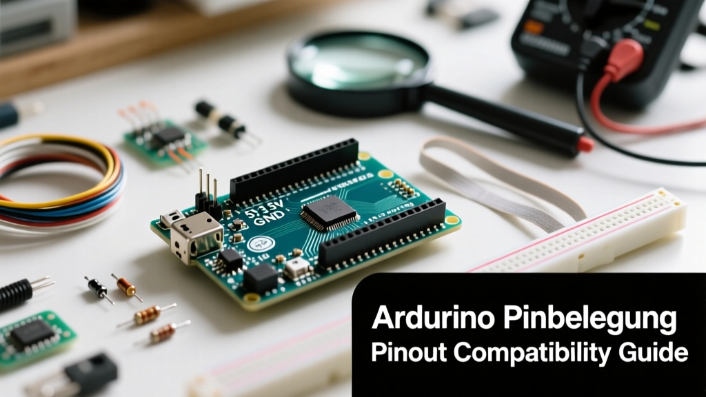

When navigating European maker communities, sourcing components from distributors like Conrad or Reichelt, or reading translated datasheets, you will frequently encounter the term Arduino Pinbelegung. In German, 'Pinbelegung' simply translates to 'pinout' or 'pin assignment.' However, understanding the physical Pinbelegung is only the first step in embedded design; the true challenge for electrical engineers and DIYers lies in cross-board compatibility. A shield designed for an UNO R3 might physically fit a Mega 2560 or an UNO R4, but the underlying pin mapping, logic levels, and internal bus architectures can cause catastrophic hardware failures if ignored.
This comprehensive compatibility guide bridges the gap between physical footprints and silicon realities, ensuring your next microcontroller project integrates flawlessly regardless of the documentation's language or origin.
The Anatomy of an Arduino Pinbelegung
The baseline for almost all Arduino-compatible shield ecosystems is the UNO R3 form factor. The physical header layout consists of 14 digital I/O pins and 6 analog input pins. However, the electrical characteristics behind these headers vary wildly depending on the silicon driving them. Below is a compatibility matrix detailing the core architectures you will encounter when reviewing a Pinbelegung datasheet.
| Board Model | Microcontroller | Digital I/O | PWM Channels | Native Logic Level |
|---|---|---|---|---|
| UNO R3 | ATmega328P | 14 | 6 | 5.0V |
| Nano V3 | ATmega328P | 14 | 6 | 5.0V |
| Mega 2560 | ATmega2560 | 54 | 15 | 5.0V |
| UNO R4 Minima | Renesas RA4M1 | 14 | 6 | 5.0V (3.3V tolerant) |
Cross-Platform Shield Compatibility and Bus Relocation
The most common point of failure when adapting a Pinbelegung from one board to another is the assumption that identical physical headers mean identical internal routing. This is especially dangerous when dealing with communication buses.
The SPI Bus Mismatch
The Serial Peripheral Interface (SPI) is the primary culprit in shield incompatibility. On the standard UNO R3, the SPI bus is mapped to the digital pins: 10 (SS), 11 (MOSI), 12 (MISO), and 13 (SCK). If you review the Pinbelegung for the Arduino Mega 2560, you will find that the SPI bus is relocated to pins 50 (MISO), 51 (MOSI), 52 (SCK), and 53 (SS).
If you plug an UNO-specific SPI shield (like the classic Ethernet Shield W5100) into a Mega 2560, the shield will physically seat perfectly, but the microcontroller will fail to initialize the hardware. The workaround is to ensure your shield utilizes the 2x3 ICSP header, which maintains consistent SPI routing across almost all 5V Arduino form factors.
I2C and the R3 Revision Shift
Prior to the R3 revision, the I2C bus was strictly mapped to Analog 4 (SDA) and Analog 5 (SCL). The R3 revision introduced a dedicated I2C header near the USB port. While the ATmega328P internally still routes these to A4 and A5, newer microcontrollers like the Renesas RA4M1 on the UNO R4 have dedicated hardware I2C pins that do not map to the analog header. Modern shields rely on the dedicated R3 I2C header for cross-compatibility.
The 5V vs 3.3V Logic Level Trap
A frequent oversight when interpreting a Pinbelegung is ignoring the voltage tolerance column. The legacy Arduino ecosystem operates at 5V logic. However, the modern sensor ecosystem (including Bosch BME280s, STMicroelectronics IMUs, and high-density OLEDs) strictly requires 3.3V logic. Applying 5V to the SDA/SCL lines of a 3.3V sensor will instantly destroy its internal ESD protection diodes.
To maintain compatibility between a 5V ATmega328P and a 3.3V peripheral, you must implement bidirectional logic level shifting. There are two primary methods:
- BSS138 MOSFET Arrays: The most reliable and cost-effective method for I2C. By using N-channel MOSFETs with pull-up resistors on both the 5V and 3.3V sides, the open-drain nature of I2C is preserved. You can review the schematic breakdown in the SparkFun Logic Level Shifting Tutorial.
- CD4050B Non-Inverting Buffers: Ideal for one-way SPI or UART lines (like MOSI and SCK), but unsuitable for bidirectional I2C without complex routing.
- TXB0108 Transceivers: Texas Instruments' auto-direction sensing chips are excellent for high-speed SPI but often fail with I2C due to the specific pull-up requirements of the I2C specification.
Translating German Schematics: Pinbelegung Glossary
If you are sourcing custom PCBs or reading documentation from European engineering firms, you will need to map German schematic terminology to standard Arduino pin definitions. Keep this glossary handy when deciphering a foreign Pinbelegung diagram:
- Eingang (E): Input (Digital or Analog)
- Ausgang (A): Output
- Masse / GND: Ground (0V reference)
- Betriebsspannung (VCC): Operating Voltage (Usually 5V or 3.3V)
- Interrupt-Eingang: Interrupt Pin (Usually mapped to D2 or D3 on ATmega328P)
- Analog-Digital-Wandler (ADC): Analog-to-Digital Converter pins (A0-A5)
Pro Tip: When reading German datasheets for relay modules, look for the term 'Optokoppler' (optocoupler). This indicates the module features optical isolation, meaning the Pinbelegung for the control signal requires a current-sinking (active LOW) configuration rather than a standard voltage-high trigger.
Silicon Shifts: UNO R3 vs UNO R4 ADC Mapping
Even when the physical Pinbelegung remains 100% backward compatible, the silicon beneath the headers can alter your code's behavior. The transition from the Arduino UNO R3 to the UNO R4 Minima is a prime example.
The ATmega328P features a 10-bit ADC, meaning analogRead() returns values from 0 to 1023. The Renesas RA4M1 on the R4 features a 14-bit ADC. While the Arduino IDE core attempts to scale this down to 10-bit for legacy compatibility, advanced users utilizing direct register manipulation or high-precision DAQ (Data Acquisition) shields will notice significant discrepancies in resolution and sampling rates. Furthermore, the R4 introduces a true 12-bit DAC (Digital-to-Analog Converter) on pin A0, a feature entirely absent from the legacy ATmega Pinbelegung, allowing for true analog voltage output rather than PWM simulation.
Clone Board Quirks: CH340 vs ATmega16U2
When purchasing third-party clone boards, the main microcontroller (ATmega328P) usually retains the exact same Pinbelegung as the official boards. However, the USB-to-UART bridge chip is frequently swapped from the official ATmega16U2 to the WCH CH340G to reduce manufacturing costs.
While this does not affect your digital I/O pins, it introduces two compatibility issues:
- Driver Dependencies: The CH340 requires specific OS-level drivers on Windows and macOS, which can cause port enumeration failures in the IDE.
- Physical Z-Height: The CH340G is often housed in a larger SOIC-16 package compared to the QFN package of the 16U2. This can increase the physical height of the USB-B port or surrounding components, causing mechanical interference with the bottom PCB of stacked shields.
Summary: Best Practices for Pin Mapping
Mastering the Arduino Pinbelegung requires looking past the physical silk-screen labels printed on the PCB. Always verify the logic voltage of your target microcontroller against your peripherals. When migrating code between form factors like the UNO and Mega, rely on the ICSP header for SPI communications and the dedicated R3 header for I2C. Finally, when dealing with international documentation or clone boards, verify the underlying silicon and USB-UART bridges to ensure your software stack aligns with the physical hardware reality.