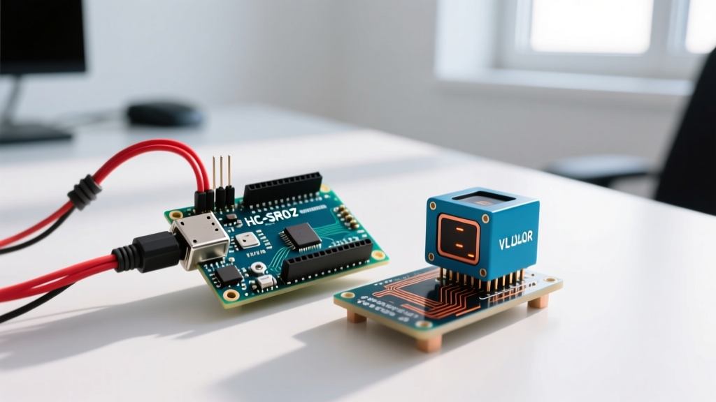

The Legacy Bottleneck: Why the ATmega328P ADC Falls Short
For over a decade, the standard Arduino Uno R3 and its ATmega328P microcontroller have been the default starting point for electronics hobbyists. However, as sensor technology and project requirements have evolved in 2026, the limitations of the native analogRead() function have become a significant bottleneck. The ATmega328P features a 10-bit Successive Approximation Register (SAR) Analog-to-Digital Converter (ADC). This yields a maximum resolution of 1,024 discrete steps. When referenced to a 5V supply, each step represents approximately 4.88mV. For basic potentiometer readings or simple light sensors, this is adequate. For precision load cells, medical-grade biometric sensors, or high-fidelity audio sampling, a 4.88mV noise floor and a maximum sample rate of roughly 9.6 kSPS (kilo-samples per second) are entirely insufficient.
Expert Insight: The ATmega328P ADC also suffers from significant Integral Non-Linearity (INL) and requires a low-impedance source (under 10kΩ) to properly charge its internal sample-and-hold capacitor within the 1.5 ADC clock cycles allocated for acquisition. Failing to buffer high-impedance sensors results in wildly inaccurate readings.
If your project demands higher precision, lower noise, or faster sampling rates, it is time to migrate your analog input in Arduino ecosystems to a more capable architecture. This guide outlines two primary upgrade paths: integrating an external 16-bit Delta-Sigma ADC, or migrating to a modern high-performance microcontroller board.
Migration Path A: External 16-Bit ADC (Texas Instruments ADS1115)
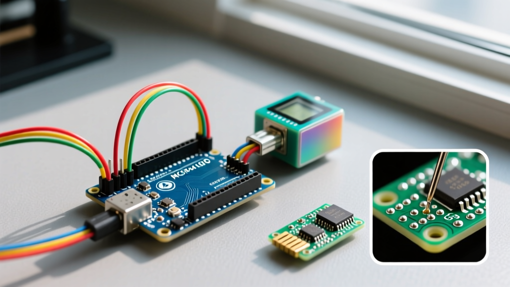
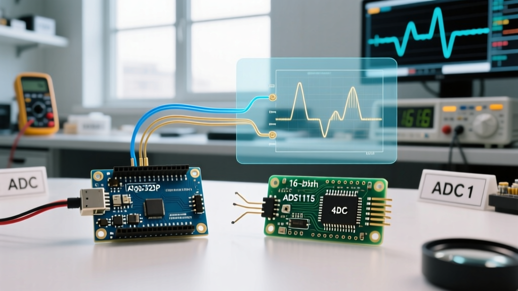
The most common and cost-effective way to upgrade your analog input in Arduino projects without changing your primary microcontroller is to bypass the internal ADC entirely and use an external IC. The Texas Instruments ADS1115 is a 16-bit, 4-channel, Delta-Sigma ADC that communicates via I2C. In 2026, breakout boards from manufacturers like Adafruit and SparkFun remain widely available, typically priced between $4.95 and $6.50.
Hardware Integration and Wiring
Migrating to the ADS1115 requires shifting from simple analog pin wiring to an I2C bus architecture. The module features four analog inputs (A0-A3), which can be configured as four single-ended inputs or two differential pairs.
- VDD: Connect to 3.3V or 5V (matches your MCU logic level).
- GND: Connect to system ground. Critical: Use a star-ground topology to prevent 50/60Hz mains hum from corrupting your 16-bit resolution.
- SCL / SDA: Connect to the I2C clock and data pins. You must install 4.7kΩ pull-up resistors to the logic voltage if your breakout board does not have them populated. For 400kHz Fast-Mode I2C, drop these to 2.2kΩ.
- ADDR: Ties to GND for the default I2C address of
0x48.
Configuring the Programmable Gain Amplifier (PGA)
The true power of the ADS1115 lies in its internal PGA, which allows you to scale the input voltage range to maximize resolution. Unlike the fixed 0-5V range of the Uno, the ADS1115 offers six selectable ranges:
- ±6.144V: 1 bit = 0.1875mV (Default, but note that VDD limits actual input to 5V).
- ±4.096V: 1 bit = 0.125mV.
- ±2.048V: 1 bit = 0.0625mV (Ideal for standard 3.3V sensors).
- ±1.024V: 1 bit = 0.03125mV (Excellent for load cells and strain gauges).
- ±0.512V: 1 bit = 0.015625mV.
- ±0.256V: 1 bit = 0.0078125mV (Requires extremely clean signal paths).
Migration Path B: Native High-Speed MCU (Teensy 4.1)
If your project requires high-speed sampling—such as digital signal processing (DSP), vibration analysis, or software-defined radio—an external I2C ADC will bottleneck your system. The I2C bus and the ADS1115's maximum 860 SPS (samples per second) are too slow. In this scenario, migrating the entire brain of your project to a board like the Teensy 4.1 (priced at $32.95) is the superior engineering choice.
The Teensy 4.1 utilizes an NXP i.MX RT1062 ARM Cortex-M7 processor running at 600 MHz. More importantly for analog tasks, it features dual 12-bit SAR ADCs capable of sampling at up to 1 MSPS (million samples per second). While 12-bit resolution (4,096 steps) is technically lower than the ADS1115's 16-bit output, the massive oversampling capabilities and 1 MSPS speed allow you to use software-based oversampling and decimation to achieve 16-bit effective resolution while maintaining high bandwidth.
The 3.3V Logic Caveat
When migrating from a 5V Arduino Uno to a Teensy 4.1 or similar modern ARM board, remember that the analog inputs are strictly limited to 3.3V. Feeding a 5V sensor signal directly into a Teensy analog pin will permanently damage the silicon. You must implement a precision voltage divider using 0.1% tolerance resistors, or use an active op-amp level-shifter circuit to scale your 0-5V signals down to 0-3.3V.
Architecture Comparison Matrix
To help you decide which migration path fits your specific 2026 project requirements, review the technical specifications below:
| Feature | Arduino Uno R3 (Legacy) | ADS1115 (External I2C) | Teensy 4.1 (Native ARM) | ESP32-S3 (Native Wi-Fi) |
|---|---|---|---|---|
| Resolution | 10-bit (1,024 steps) | 16-bit (65,536 steps) | 12-bit (4,096 steps) | 12-bit (4,096 steps) |
| Max Sample Rate | ~9.6 kSPS | 860 SPS | 1,000,000 SPS | ~83 kSPS |
| Architecture | SAR | Delta-Sigma | Dual SAR | SAR |
| Input Voltage | 0 - 5.0V | 0 - VDD (Max 5.5V) | 0 - 3.3V | 0 - 3.3V |
| Best Use Case | Basic prototyping | High-precision, slow DC | High-speed DSP / Audio | IoT with basic sensing |
| Approx. Cost (2026) | $27.50 (Official) | $4.95 (Breakout) | $32.95 (Board) | $8.00 (Dev Board) |
Real-World Failure Modes and Edge Cases
Upgrading your analog input in Arduino environments introduces new complexities. Be aware of these common failure modes encountered in professional and advanced hobbyist deployments:
1. ESP32-S3 ADC Non-Linearity
Many makers attempt to migrate to the ESP32-S3 for its built-in Wi-Fi and 12-bit ADC. However, the ESP32 SAR ADC is notorious for severe non-linearity at the extreme ends of its range. Readings below 0.15V and above 3.15V are highly inaccurate and non-monotonic. If your sensor operates in these boundary regions, you must use an op-amp to shift and scale the signal into the 0.5V - 2.8V linear sweet spot, or revert to an external ADS1115.
2. I2C Bus Capacitance and Noise
When using the ADS1115 in electrically noisy environments (e.g., near stepper motors or switching power supplies), the I2C bus can suffer from capacitive loading. The I2C specification limits bus capacitance to 400pF. If your wiring is long or unshielded, the signal edges will round off, causing I2C ACK failures and frozen sketches. Always use twisted-pair cables for I2C runs exceeding 30cm, and consider adding a dedicated I2C bus extender like the PCA9600 for industrial applications.
3. Ground Loops in Differential Measurements
The ADS1115 supports differential measurements, which are excellent for rejecting common-mode noise. However, if the ground potential of your sensor differs from the Arduino ground by more than a few millivolts, it can skew the differential reading. Ensure that the analog ground of the sensor and the GND pin of the ADS1115 are tied together at a single physical point to eliminate ground loop currents.
Code Migration Strategy: Moving to Non-Blocking Reads
When you upgrade from the native analogRead() to an external ADS1115, your code must change. The analogRead() function is blocking; it halts the MCU until the conversion is complete. The ADS1115, communicating over I2C at 128 SPS (default), takes roughly 7.8 milliseconds per read. Calling it in a fast loop() will severely degrade your system's responsiveness.
To migrate properly, implement a non-blocking state machine or utilize the Adafruit_ADS1X15 library's interrupt (ALRT) pin. By configuring the ADS1115's LO_THRESH and HI_THRESH registers, you can trigger a hardware interrupt on the Arduino only when a new conversion is ready. This allows your main loop to handle motor control, display updates, or network communication without being stalled by ADC acquisition times.
Summary
Migrating your analog input in Arduino projects from the legacy 10-bit internal ADC to a 16-bit external Delta-Sigma converter or a high-speed 12-bit ARM MCU is a necessary step for any serious precision or DSP application. By understanding the trade-offs between resolution, sample rate, and bus topology, you can select the exact architecture required to eliminate noise, increase fidelity, and future-proof your hardware designs for 2026 and beyond.