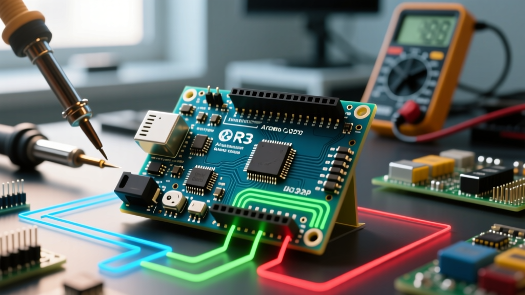

Understanding the Arduino Uno R3 Schema: A Beginner's Blueprint
When you first dive into microcontroller projects, the physical board is all you see. But to truly master hardware debugging, custom shield design, or advanced wiring, you need to understand what lies beneath the fiberglass. This is where the Arduino Uno R3 schema (more commonly referred to in English as the schematic or circuit diagram) becomes your most valuable tool. In 2026, while newer boards like the Uno R4 Minima and Wi-Fi have entered the market, the classic Uno R3 remains the undisputed king of beginner education and legacy DIY projects, largely due to its robust, open-source hardware design.
For a beginner, 'schema' might sound like an intimidating engineering term. In reality, it is simply a visual map of how every component on the board connects electrically. Whether you are trying to figure out why your 5V rail is dead, or you need to know which pins support hardware PWM, reading the Uno R3 schematic is the fastest way to find the answer. In this guide, we will decode the official Arduino Uno R3 schema, break down its core architectural blocks, and teach you how to use this blueprint for real-world troubleshooting.
Decoding the Core Architecture Blocks
The official Arduino Uno Rev3 documentation divides the board's schema into three primary functional zones. Understanding these zones is the first step to reading the schematic like an electrical engineer.
1. The Main Microcontroller Zone
At the heart of the schema sits the ATmega328P-PU, a 28-pin DIP (Dual In-line Package) integrated circuit manufactured by Microchip (formerly Atmel). This chip handles all your code execution, digital I/O, and analog-to-digital conversions. According to the official Microchip ATmega328P product specifications, this chip operates at a maximum clock speed of 20MHz, but the Uno R3 schema clocks it at 16MHz using a 16MHz quartz crystal (Y1) and two 22pF load capacitors (C4 and C5).
2. The USB-to-Serial Interface Zone
Because the ATmega328P lacks native USB hardware, the schema includes a secondary, smaller microcontroller dedicated solely to translating USB signals from your computer into UART (Serial) signals the main chip can understand. On a genuine Uno R3, this is the ATmega16U2-MU (a 32-pin QFN package). This chip is also responsible for the automatic reset circuit that allows the Arduino IDE to upload code without you having to manually press the reset button.
3. The Power Management Zone
The power schema handles stepping down raw voltage from the barrel jack or Vin pin into stable logic levels. It utilizes an NCP1117ST50T3G linear voltage regulator to provide the 5V rail, and an LP2985-33DBVR to provide the 3.3V rail.
Component Reference Designator Map
When looking at the official PDF schema, you will see letters and numbers next to every part. Here is a quick-reference table to help you map the schematic designators to the physical components on your board.
| Schematic Ref | Component Name / Value | Function on the Board |
|---|---|---|
| U1 | ATmega16U2-MU | USB-to-Serial bridge controller |
| U2 | ATmega328P-PU | Main microcontroller (brains) |
| IC1 | NCP1117ST50T3G | 5V Linear Voltage Regulator |
| U4 | LP2985-33DBVR | 3.3V Linear Voltage Regulator |
| F1 | RXE040 (Polyfuse) | Resettable PTC fuse (USB overcurrent protection) |
| D1 | M7 Diode | Reverse polarity protection for the barrel jack |
| Y1 | 16MHz Crystal | Main clock oscillator for U2 |
Mapping the Pinout Schema for Practical Wiring
Beginners often search for the 'Arduino Uno R3 schema' when they actually need a pinout map. The schematic reveals the hidden capabilities of the header pins that aren't always obvious from the silkscreen on the board.
Digital I/O and PWM Capabilities
The schema shows that the ATmega328P has 14 digital I/O pins (D0 to D13). However, not all pins are created equal. By tracing the lines on the schematic to the microcontroller's internal timer modules, we can identify the hardware Pulse Width Modulation (PWM) pins. These are marked with a tilde (~) on the board silkscreen.
- PWM Pins: 3, 5, 6, 9, 10, and 11. (Use these for motor speed control or LED dimming).
- UART / Serial Pins: 0 (RX) and 1 (TX). These are physically wired to the ATmega16U2 USB chip. Warning: Connecting external devices here can interfere with USB code uploads.
- SPI Bus: 11 (MOSI), 12 (MISO), 13 (SCK). Also broken out to the 6-pin ICSP header.
- I2C Bus: A4 (SDA) and A5 (SCL). Duplicated on the separate header added in the Rev3 schema update.
Analog Inputs vs. Digital Outputs
The schema designates pins A0 through A5 as analog inputs, routed to the ATmega328P's internal 10-bit ADC (Analog-to-Digital Converter). A common beginner mistake is trying to use these pins for analog output. The Uno R3 schema does not include a DAC (Digital-to-Analog Converter); therefore, A0-A5 can only read analog voltages (0-5V), not output them. Furthermore, A6 and A7 exist on the physical ATmega328P chip but are not routed to the Uno R3 header pins in the schematic.
CRITICAL CURRENT LIMIT: The ATmega328P datasheet specifies an absolute maximum DC current per I/O pin of 40mA. However, the safe continuous operating limit recommended by engineers is 20mA per pin, with a total combined limit of 200mA for all VCC/GND pins. Never wire a high-draw component like a DC motor directly to an I/O pin; always use a MOSFET or BJT transistor as a switch.
The Power Supply Schema: Protection and Rails
One of the most vital sections of the Arduino Uno R3 schema for troubleshooting is the power input circuit. Understanding how power flows from the barrel jack to the 5V pin can save you from destroying your board.
- Reverse Polarity Protection (D1): If you accidentally use a power adapter with a center-negative plug instead of the required center-positive plug, the M7 diode blocks the reverse current, preventing catastrophic failure of the voltage regulator.
- Voltage Regulator (IC1): The NCP1117 takes the raw input voltage (recommended 7V to 12V) and drops it to a stable 5V. Because it is a linear regulator, excess voltage is burned off as heat. If you input 12V and draw 500mA, the regulator must dissipate 3.5 Watts of heat, which will trigger its internal thermal shutdown.
- USB Polyfuse (F1): The RXE040 is a resettable PTC fuse placed in series with the USB VBUS line. If your USB hub or computer port tries to pull more than 500mA, the fuse heats up and increases its resistance, effectively cutting off the power to protect your computer's motherboard.
Genuine vs. Clone Schematic Differences
As of 2026, genuine Arduino Uno R3 boards retail for approximately $27.99, while third-party clones can be found for $8.00 to $12.00. While clones are excellent for learning, their internal schemas often differ from the official open-source design in one major way: the USB-to-Serial chip.
To cut costs, most clone manufacturers replace the ATmega16U2 with a CH340G or CH340C chip. If you are looking at the official Arduino schema and trying to trace the USB D+ and D- lines, they will not match your physical clone board. The CH340 is a dedicated, single-purpose USB-UART bridge, meaning it lacks the firmware-flashable nature of the 16U2, but it performs the exact same serial communication duties. You will simply need to install the CH340 driver on your Windows or macOS machine to get it recognized by the Arduino IDE.
How to Troubleshoot Using the Schema and a Multimeter
Learning to read schematics is best applied practically. If your Uno R3 suddenly stops powering on, follow this schema-guided troubleshooting flow using a standard digital multimeter:
Step 1: Test the USB Polyfuse (F1)
Set your multimeter to continuity mode (the diode/beep symbol). Place the probes on either side of the F1 polyfuse near the USB port. If it beeps, the fuse is intact. If it reads 'OL' (Open Line) and the board was recently connected to a high-draw shield, the fuse has tripped. Unplug the board and wait 10 minutes for it to cool and reset.
Step 2: Check the 5V Regulator Output (IC1)
Power the board via the barrel jack with a 9V adapter. Set your multimeter to DC Voltage. Place the black probe on any GND pin and the red probe on the output leg of the NCP1117 regulator (or simply on the '5V' header pin). You should read exactly 4.95V to 5.05V. If you read 0V, check if the input voltage is reaching the regulator's input pin. If input is present but output is 0V, the regulator is dead and must be desoldered and replaced.
Step 3: Verify the Crystal Oscillator (Y1)
If the board powers on, the 'L' LED blinks, but code refuses to upload or execute, the 16MHz crystal might be damaged (common if the board is dropped). While an oscilloscope is best for testing crystals, you can use a multimeter's frequency setting (Hz) on the crystal's pads. You should see a reading hovering near 16,000,000 Hz. If it reads 0, the clock circuit is broken.
Frequently Asked Questions
Can I power the Uno R3 by feeding 5V directly into the 5V pin?
Yes, the schema shows that the 5V header pin bypasses the NCP1117 voltage regulator and feeds directly into the ATmega328P's VCC rail. However, doing this bypasses the board's overvoltage and reverse polarity protection. Only do this if your external 5V source is highly regulated and clean.
Where is the EEPROM memory on the schematic?
You will not find a separate EEPROM chip on the Uno R3 schema. The ATmega328P contains 1KB of internal EEPROM built directly into the silicon die, alongside its 32KB of Flash memory and 2KB of SRAM.
What does the 'IOREF' pin do in the Rev3 schema?
Added in the Revision 3 schematic update, the IOREF pin outputs the exact logic voltage the microcontroller is currently running at (5V on the Uno). This allows third-party shields to read this pin and automatically switch their internal logic level translators between 3.3V and 5V operation safely.
For further reading on interpreting electronic blueprints, the SparkFun guide on reading schematics is an excellent companion resource to keep open in a separate tab while you analyze your Uno R3. Mastering the schema transforms you from a simple code-copier into a true hardware engineer capable of designing custom PCBs and diagnosing complex electrical faults.