
Decoding the Arduino Uno R3 Diagram and Ecosystem Architecture
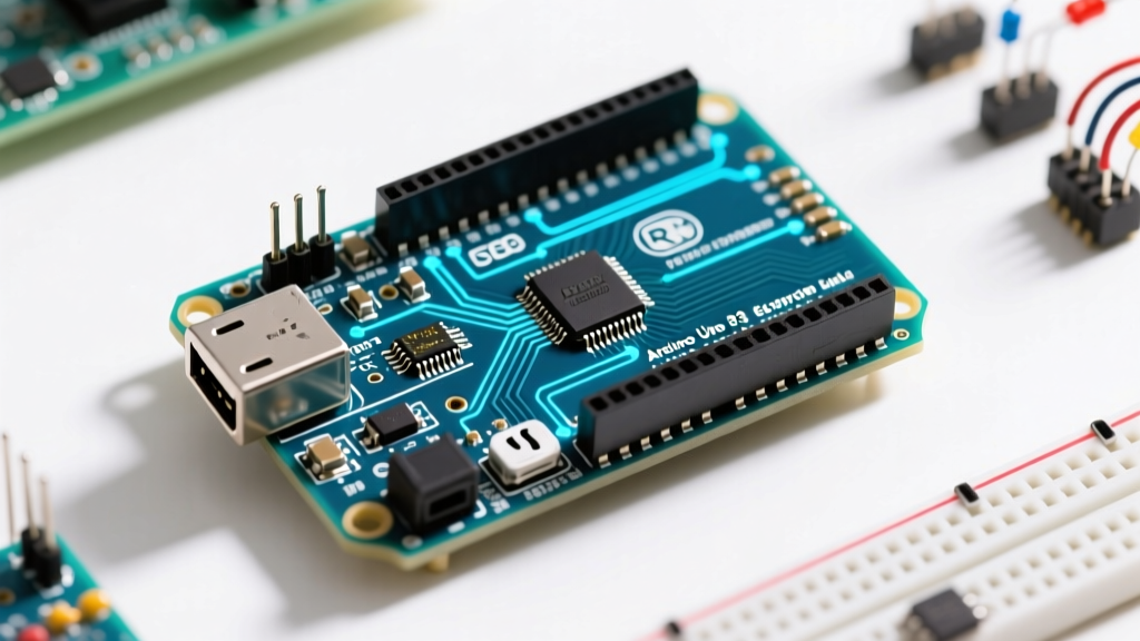
Even as we navigate the advanced microcontroller landscape of 2026, the Arduino Uno R3 remains the undisputed baseline of the maker ecosystem. Whether you are designing a custom shield, troubleshooting a bootloop, or integrating legacy hardware into a modern IoT stack, understanding the Arduino Uno R3 diagram is mandatory. The schematic is not just a map of copper traces; it is the blueprint that dictates how thousands of third-party shields, sensors, and software libraries interact with the board.
While newer platforms like the ESP32-S3 or the Arduino Uno R4 Minima offer superior processing power, the Uno R3’s physical layout and electrical characteristics have become the industry standard for prototyping. In this ecosystem overview, we will dissect the official schematic, analyze critical power delivery limitations, and map the pinout architecture to real-world compatibility scenarios.
Core Schematic Blocks: Inside the ATmega328P Architecture
When you examine the official Arduino Uno R3 documentation, the schematic divides neatly into four primary functional blocks. Understanding these blocks is crucial for diagnosing hardware faults and designing custom carrier boards.
1. The Main Microcontroller (ATmega328P-PU)
At the heart of the board sits the Microchip (formerly Atmel) ATmega328P-PU in a 28-pin DIP package. This 8-bit AVR microcontroller operates at 16 MHz, driven by a dedicated quartz crystal oscillator (Y1) with a standard tolerance of ±30ppm. The DIP package is a deliberate ecosystem choice; it allows users to physically remove the chip, program it on the Uno, and transplant it into a standalone breadboard circuit—a workflow that surface-mount variants like the Nano or Pro Mini do not easily support.
2. The USB-to-Serial Bridge
The Uno R3 schematic utilizes a secondary microcontroller, the ATmega16U2, to handle USB-to-Serial conversion. Unlike the FTDI chips used on older Duemilanove boards, the 16U2 can be reprogrammed via DFU (Device Firmware Upgrade) mode. This allows the genuine Uno R3 to act as a native USB HID device (like a keyboard or mouse) without additional hardware, a feature heavily leveraged in accessibility and macro-pad projects.
3. Power Regulation and Distribution
The power section relies on an NCP1117ST50T3G linear voltage regulator (LDO) to step down input voltage from the barrel jack or VIN pin to a stable 5V. A secondary LDO handles the 3.3V rail, which is strictly limited to 50mA. This asymmetry in power delivery is a frequent trap for beginners integrating modern 3.3V sensors.
4. Reset and Auto-Programming Circuitry
A 100nF capacitor (C5) bridges the DTR (Data Terminal Ready) line from the 16U2 to the RESET pin of the ATmega328P. This capacitive coupling is the secret to the Arduino ecosystem’s frictionless upload process, allowing the IDE to trigger a hardware reset precisely milliseconds before pushing compiled hex data via the serial bootloader.
The USB Bridge Divide: Genuine vs. Clone Ecosystems
The most significant deviation in the broader Uno R3 ecosystem is the USB-to-Serial bridge. While the genuine Arduino Uno R3 (retailing around $27.60) uses the ATmega16U2, the vast majority of sub-$12 clones utilize the WCH CH340G or Silicon Labs CP2102 chips.
Ecosystem Impact: The CH340G is a dedicated, hardwired USB-to-UART chip. It cannot be reflashed to act as a native USB HID device. Furthermore, while Windows 11 and modern Linux kernels in 2026 include native CH340 drivers, macOS users occasionally still face kernel extension (kext) conflicts when using unsigned clone drivers, leading to serial port enumeration failures.
Power Delivery Limits and Thermal Failure Modes
A deep dive into the Arduino Uno R3 diagram reveals a critical vulnerability in the power regulation stage that plagues many intermediate projects. The NCP1117 5V LDO is rated for 1A of continuous current. However, the physical SOT-223 package on the Uno PCB lacks an adequate thermal heatsink or dedicated copper pour.
Consider a common scenario: powering the Uno via the barrel jack with a 12V wall adapter while drawing 300mA for a strip of WS2812B LEDs connected to the 5V pin.
- Voltage Drop: 12V (Input) - 5V (Output) = 7V
- Power Dissipation: 7V × 0.3A = 2.1 Watts
- Thermal Resistance ($\theta_{JA}$): ~100°C/W (Junction-to-Ambient without forced air or heavy copper)
- Temperature Rise: 2.1W × 100°C/W = 210°C
Adding the 210°C rise to a 25°C ambient room temperature yields a theoretical junction temperature of 235°C. Long before this, the LDO will hit its internal thermal shutdown threshold (typically 155°C), causing the board to brownout and reset continuously. If the thermal pad is poorly soldered—a common defect in cheap clones—the chip will suffer catastrophic thermal failure. Actionable Advice: If your project requires more than 150mA at 5V, bypass the onboard LDO entirely and supply regulated 5V directly to the 5V pin, or use a dedicated buck converter module.
Pinout Architecture and Shield Compatibility Matrix
The physical pinout of the Uno R3 is the foundation of the Arduino shield ecosystem. The spacing and grouping of headers were standardized to ensure that a motor shield designed in 2012 still physically mates with a board purchased today. Below is a functional mapping of the pinout as it relates to modern ecosystem integrations.
| Pin Group | Function / Protocol | Ecosystem Use Case & Constraints |
|---|---|---|
| D0 (RX), D1 (TX) | Hardware UART (Serial) | Reserved for USB communication. Using these for external modules (like Bluetooth HC-05) requires disconnecting them during code uploads. |
| D2, D3 | External Interrupts (INT0, INT1) | Critical for rotary encoders and flow sensors. D3 also supports PWM output. |
| D3, D5, D6, D9, D10, D11 | PWM Output (~490Hz or ~980Hz) | Used for LED dimming and basic servo control. Note: D5 and D6 operate at 980Hz, while others default to 490Hz. |
| D10, D11, D12, D13 | SPI Bus (SS, MOSI, MISO, SCK) | High-speed communication for SD cards, RFID (RC522), and TFT displays. D13 is tied to the onboard LED. |
| A4 (SDA), A5 (SCL) | I2C Bus (Wire Library) | The backbone of modern sensor integration (BME280, OLEDs). Duplicated on the separate 6-pin header for shield routing. |
| A0 - A5 | 10-bit ADC (Analog Input) | Reads 0-5V with ~4.9mV resolution. A4/A5 can be repurposed as digital I/O if I2C is unused. |
Ecosystem Positioning: Uno R3 vs. Modern Alternatives
While the Arduino Uno R3 diagram is a masterclass in 8-bit simplicity, the 2026 maker ecosystem offers powerful alternatives. When should you stick to the R3, and when should you migrate?
| Feature | Arduino Uno R3 | Arduino Uno R4 Minima | ESP32 DevKit V1 |
|---|---|---|---|
| Core MCU | ATmega328P (8-bit AVR) | Renesas RA4M1 (32-bit ARM Cortex-M4) | Xtensa LX6 (32-bit Dual-Core) |
| Clock Speed | 16 MHz | 48 MHz | 240 MHz |
| SRAM | 2 KB | 32 KB | 520 KB |
| Operating Voltage | 5V (Tolerant) | 5V (Tolerant) | 3.3V (Strict) |
| Connectivity | None (requires shields) | None (requires shields) | Native Wi-Fi & Bluetooth |
| Typical Price (2026) | $27.60 (Genuine) / $11 (Clone) | $20.00 | $6.50 - $9.00 |
| Primary Ecosystem Role | Education, 5V legacy shields, basic robotics. | Advanced DSP, floating-point math, 12-bit DAC. | IoT, edge computing, high-speed data logging. |
When to Upgrade from the R3
If your project requires heavy floating-point math (like Kalman filtering for IMU sensor fusion) or native wireless telemetry, the ATmega328P will bottleneck your development. The ESP32 is the logical leap for IoT, but remember that its 3.3V logic means you must use level shifters when interfacing with the massive back-catalog of 5V Arduino shields designed for the Uno R3 pinout.
Frequently Asked Questions
Why are there two extra pins on the Uno R3 diagram compared to older versions?
The "R3" (Revision 3) update added an IOREF pin and an unconnected spare pin next to the RESET pin. IOREF allows shields to read the operating voltage of the board (5V on the Uno, 3.3V on the Due) and adapt their logic levels accordingly, ensuring cross-platform shield compatibility.
Can I use the Arduino Uno R3 schematic to design my own custom PCB?
Yes. Arduino publishes the Uno R3 schematic and board files under a Creative Commons Attribution Share-Alike license. You are free to manufacture your own derivative boards, provided you do not use the trademarked "Arduino" name and logo on your custom PCBs.
What happens if I accidentally feed 5V into the 3.3V pin?
The 3.3V pin on the Uno R3 is an output from a secondary LDO, not a regulated input. Back-feeding 5V into this pin will likely destroy the LDO and potentially back-power the ATmega16U2 USB bridge chip in an unregulated state, leading to permanent hardware damage.