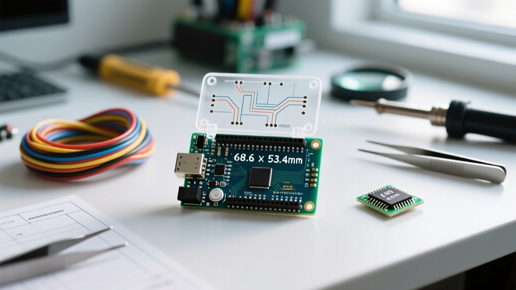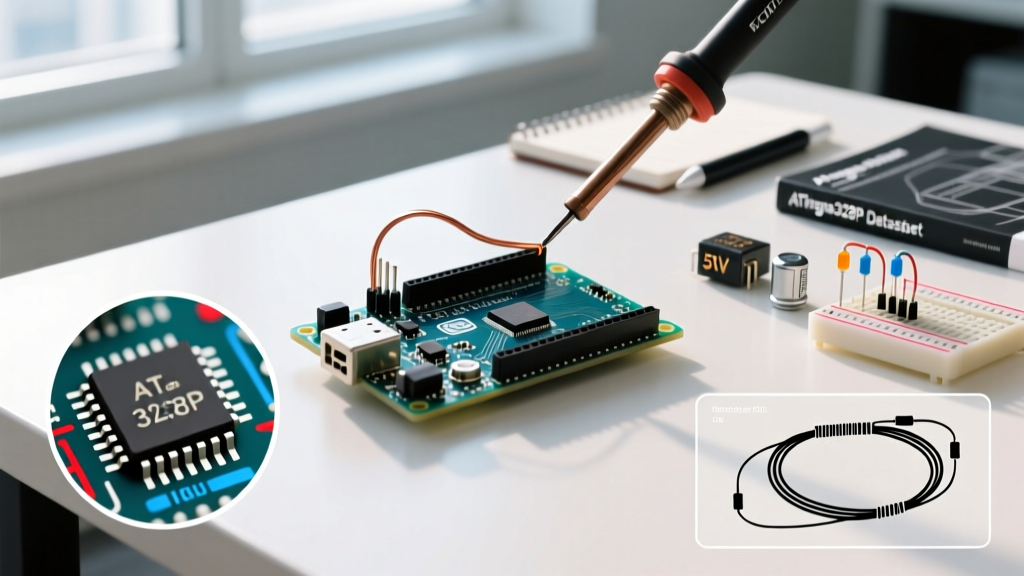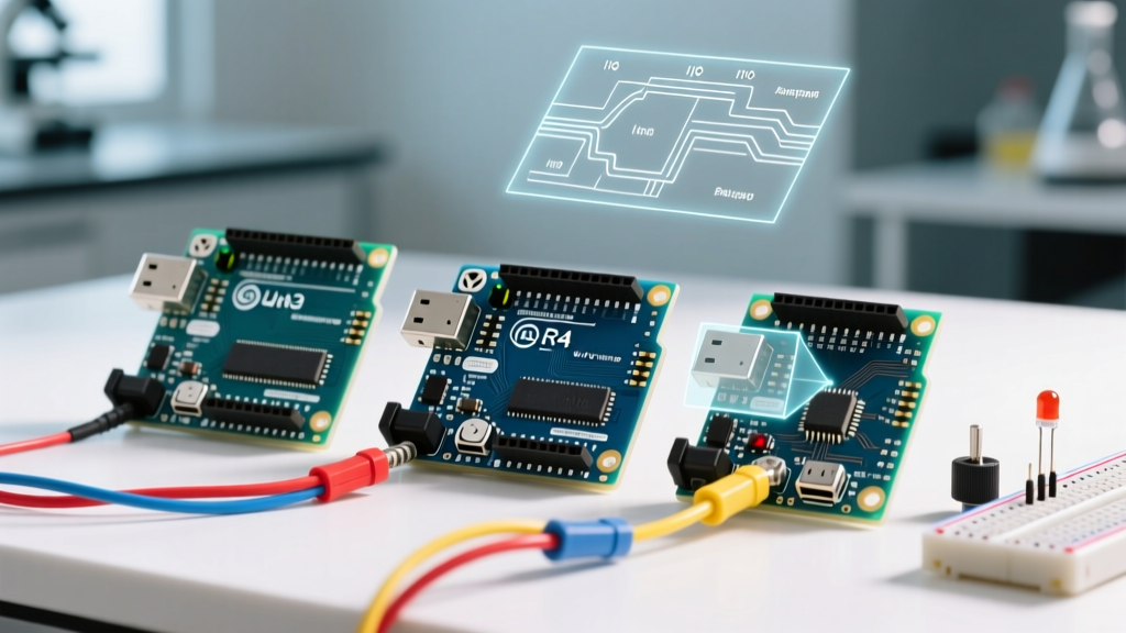

The Universal Language: Understanding the Pin Diagram of Arduino Uno
Every electronics engineer, hobbyist, and student eventually memorizes the pin diagram of Arduino Uno. It is the foundational blueprint for thousands of DIY projects, robotics platforms, and IoT prototypes. However, while the physical layout of the headers remains universally consistent across the ecosystem, the underlying hardware implementation varies drastically depending on whether you are using a $6 budget clone or a $25 premium official board.
In 2026, the market is flooded with generic ATmega328P development boards. While these budget alternatives are fantastic for simple LED blinking or basic sensor reading, they often take severe liberties with the official schematic. Conversely, premium boards—like the official Arduino Uno R3 and the modern 32-bit Arduino Uno R4 Minima—adhere strictly to reference designs, adding crucial protection circuits and advanced routing that completely change how those pins behave under stress.
This guide dissects the standard pin diagram of Arduino Uno, cluster by cluster, contrasting the harsh realities of budget clones against the engineering integrity of premium platforms.
1. The Power Cluster: VIN, 5V, 3.3V, GND, and IOREF
The power header is where budget boards most frequently fail. Looking at the pin diagram, you see VIN, 5V, 3.3V, GND, and IOREF. On paper, they all supply the correct voltages. In practice, the component selection dictates survival.
Voltage Regulation and Thermal Limits
When powering the board via the VIN pin or the barrel jack, the voltage passes through a linear regulator.
- Budget Clones ($4 - $8): Almost universally use a generic
AMS1117-5.0SMD regulator. This component lacks an adequate thermal pad on the PCB ground plane. If you draw 300mA from the 5V pin while supplying 12V to VIN, the regulator will dissipate over 2 watts of heat, triggering thermal shutdown or physically melting the solder joints. - Premium R3 ($27): Utilizes an ON Semiconductor
NCP1117ST50T3Gpaired with a robust copper pour for heat dissipation, safely handling higher voltage drops. - Premium R4 Minima ($20): Abandons the linear regulator entirely for a highly efficient switching buck converter, allowing you to draw up to 1.5A from the 5V pin without the board becoming warm to the touch.
The Missing Protection: USB VBUS Polyfuse
According to the official Uno R3 schematic, a 500mA resettable PTC polyfuse sits between the USB VBUS line and the 5V pin. Budget clones omit this $0.10 component. If you accidentally short a 5V sensor cable on a clone, you will instantly fry your computer's USB port or the board's USB-UART bridge chip.
Expert Warning: Never back-power a budget clone through the 5V pin with more than 5.5V. Clones often lack the Schottky diode that prevents reverse current from flowing back into the USB port, which can destroy your host PC's motherboard.
2. Digital I/O and PWM Mapping (D0 - D13)
The digital header contains pins D0 through D13, with PWM (Pulse Width Modulation) capabilities denoted by a tilde (~) on pins 3, 5, 6, 9, 10, and 11. While the pin diagram of Arduino Uno labels these simply as digital I/O, the internal routing reveals massive differences.
Series Resistors and Port Protection
On premium official boards, pins D0 (RX) and D1 (TX) are routed through 100-ohm series resistors before reaching the main microcontroller. This allows the USB-to-Serial chip to override the main MCU during code uploads without causing a short circuit. Budget clones frequently bypass these resistors or use incorrect values, leading to failed uploads if a shield is actively driving the TX/RX lines.
Furthermore, premium boards include clamping diodes on the I/O lines to protect against minor inductive voltage spikes from relays or motors. Clones strip these out to save fractions of a cent, meaning connecting a small DC motor directly to a PWM pin on a clone will often result in immediate silicon death due to back-EMF.
The R4 Paradigm Shift: 12-Bit DAC and Alternate Functions
If you are upgrading to the premium Arduino Uno R4 Minima, the physical pin diagram remains identical for shield compatibility, but the functional diagram changes. Pin D03 on the R4 is no longer just a standard PWM output; it is wired to a true 12-bit Digital-to-Analog Converter (DAC). This allows you to output genuine analog waveforms (like true sine waves for audio projects) directly from the pin, a feature entirely absent on the classic 8-bit ATmega328P architecture.
3. Analog Inputs and ADC Integrity (A0 - A5)
Pins A0 through A5 serve as 10-bit Analog-to-Digital Converter (ADC) inputs on classic boards. They read voltages between 0V and 5V, mapping them to integer values between 0 and 1023.
Ground Plane Isolation and Noise Floors
The accuracy of the ADC is entirely dependent on the reference voltage and the analog ground.
- The Clone Problem: Budget manufacturers use single-layer or poorly designed two-layer PCBs where digital return currents (from the microcontroller switching states) share the same ground traces as the analog reference. This introduces a noise floor of 10 to 15 LSBs (Least Significant Bits). If you are trying to read a high-precision load cell or a sensitive thermocouple amplifier, a clone's A0 pin will yield jittery, unusable data.
- The Premium Solution: Official boards utilize a split-ground plane topology, physically separating the analog ground (AGND) from the digital ground (DGND) and joining them at a single star point near the power supply. This drops the ADC noise floor to 1-2 LSBs, ensuring stable sensor readings.
4. Communication Headers: SPI, I2C, and UART
The pin diagram of Arduino Uno maps the SPI bus to pins 10 (SS), 11 (MOSI), 12 (MISO), and 13 (SCK), while the I2C bus is mapped to A4 (SDA) and A5 (SCL).
The I2C Pull-Up Resistor Omission
The I2C protocol requires pull-up resistors on the SDA and SCL lines to function correctly. The official Arduino Uno R3 documentation confirms the inclusion of 4.7kΩ pull-up resistors on the board. Budget clones almost universally omit these resistors. While the I2C bus might still work if your sensor module has its own pull-ups, daisy-chaining multiple modules on a clone without external pull-ups will result in corrupted data, bus lockups, and phantom I2C addresses.
USB-to-Serial Bridge: CH340 vs ATmega16U2
Though not explicitly part of the external header pin diagram, the USB interface is critical. Premium boards use an ATmega16U2 programmed as a USB-to-Serial converter, which supports native HID (Human Interface Device) emulation—allowing the Uno to act as a custom keyboard or mouse. Budget clones use a CH340C or CH340G chip. While the CH340 is a perfectly capable serial bridge, it strictly limits the board to standard UART communication and requires third-party driver installations on older operating systems.
Hardware Comparison Matrix: Budget Clone vs. Premium R3 vs. R4
| Feature / Pin Cluster | Budget Clone ($5) | Premium Uno R3 ($27) | Premium Uno R4 Minima ($20) |
|---|---|---|---|
| Core MCU | ATmega328P (Often refurbished) | ATmega328P (Microchip Certified) | Renesas RA4M1 (32-bit ARM Cortex-M4) |
| VIN Regulator | AMS1117 (Poor thermal handling) | NCP1117 (Optimized heat dissipation) | Switching Buck Converter (High efficiency) |
| 5V Pin Max Current | ~500mA (Thermal throttling) | ~800mA (Via VIN) | 1.5A (Robust power tree) |
| I2C Pull-ups (A4/A5) | Missing (Requires external) | 4.7kΩ Included | 4.7kΩ Included + Qwiic Connector |
| D03 Capability | Standard 8-bit PWM | Standard 8-bit PWM | 12-bit True DAC Output |
| USB Bridge | CH340C (Serial only) | ATmega16U2 (Serial + HID) | Hardware USB-C (Serial + HID + DFU) |
Final Verdict: Choosing Your Platform Based on the Pinout
Understanding the pin diagram of Arduino Uno goes far beyond memorizing which pin is SCK or where the 3.3V output lives. It requires understanding the electrical integrity behind those physical headers.
If your project involves basic digital logic, simple relays, or educational prototyping where a burnt-out $5 board is merely a minor inconvenience, a budget clone is a highly cost-effective choice. Just remember to add your own I2C pull-up resistors and never exceed 9V on the VIN pin.
However, if you are designing a permanent installation, reading sensitive analog sensors, or requiring the computational overhead and true DAC outputs of modern 32-bit architectures, the premium official boards are non-negotiable. The R4 Minima, in particular, represents the ultimate evolution of the classic Uno pin diagram, offering backward-compatible shield support while delivering vastly superior power regulation and signal integrity for demanding 2026 engineering projects.