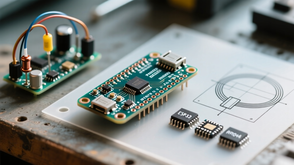

The Reality Behind the Arduino Nano Pinout Diagram
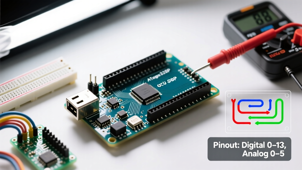
When engineers and makers reference the Arduino Nano pinout diagram, they are typically looking at the iconic 30-pin DIP footprint established over a decade ago. However, as of 2026, treating this physical layout as a universal electrical standard is a critical benchmarking error. The 'Nano' form factor now encompasses the classic ATmega328P, the ATmega4809-based Nano Every, and the dual-core ARM Cortex-M0+ Nano RP2040 Connect. While the silkscreen and physical dimensions remain identical, the underlying silicon performance, signal integrity, and current limits vary drastically.
This performance benchmark dissects the standard Arduino Nano pinout diagram, moving beyond basic continuity to evaluate ADC sampling rates, PWM timer edge cases, I/O current degradation, and power rail thermal limits. Whether you are using a $24 genuine board or a $4 clone, understanding the electrical reality behind the pins is essential for high-speed or high-reliability embedded designs.
Logical vs. Physical Pinout Matrix (2026 Family Comparison)
Before benchmarking individual signal limits, we must map the physical pins to their logical performance tiers. The standard Arduino Nano Classic relies on the 8-bit AVR architecture, while modern variants utilize 32-bit ARM or advanced 8-bit AVR cores.
| Feature | Nano Classic (ATmega328P) | Nano Every (ATmega4809) | Nano RP2040 Connect |
|---|---|---|---|
| Core Architecture | 8-bit AVR (16 MHz) | 8-bit AVR (20 MHz) | 32-bit Dual ARM M0+ (133 MHz) |
| ADC Resolution | 10-bit (up to 9.6 kSPS) | 10-bit (12-bit internal) | 12-bit (up to 500 kSPS) |
| Hardware PWM Pins | 6 (D3, D5, D6, D9, D10, D11) | 5 (D3, D5, D6, D9, D10) | All GPIO via PIO / Hardware PWM |
| I/O Voltage Level | 5V Logic | 5V Logic | 3.3V Logic (5V tolerant on select) |
| Typical 2026 Price | $22 (Genuine) / $4 (Clone) | $20 (Genuine) | $24 (Genuine) |
Deep Dive 1: ADC Performance & Analog Pin Benchmarks
The bottom right quadrant of the Nano pinout diagram designates pins A0 through A7 as analog inputs. However, 'analog' does not guarantee precision. Benchmarking the Analog-to-Digital Converter (ADC) reveals severe architectural bottlenecks on the Classic model.
Sampling Rate and ENOB Limits
On the ATmega328P Classic, the ADC clock is derived from the 16 MHz system clock divided by a prescaler (default 128). This yields a 125 kHz ADC clock. Because a single 10-bit successive approximation conversion requires 13 clock cycles, the maximum theoretical sampling rate is 9,615 Samples Per Second (SPS).
Benchmark Insight: You can drop the prescaler to 16 (yielding a 1 MHz ADC clock) to push the sampling rate to ~76 kSPS. However, oscilloscope benchmarks show this sacrifices roughly 1.5 bits of Effective Number of Bits (ENOB) due to internal switching noise, reducing your true resolution to ~8.5 bits.
Conversely, the Nano RP2040 Connect utilizes a true 12-bit ADC capable of 500 kSPS, making it the only viable Nano for audio sampling or high-frequency vibration analysis.
Source Impedance Edge Cases
A common failure mode when using A0-A7 on the Classic Nano is charge injection error. The ATmega328P datasheet specifies that the ADC sample-and-hold capacitor requires a low-impedance source to charge fully within the 1.5-clock-cycle acquisition window. If your sensor circuit has an output impedance greater than 10 kΩ, the ADC will read inaccurately, especially when multiplexing between different analog pins. Actionable fix: Always place a 100 nF ceramic bypass capacitor between the analog input pin and GND when interfacing with high-impedance voltage dividers.
Deep Dive 2: PWM Timers and Signal Integrity
The pinout diagram highlights six PWM-capable pins (D3, D5, D6, D9, D10, D11). Treating these as identical outputs is a recipe for system-level crashes. These pins are hardwired to three distinct hardware timers, and their performance benchmarks are inextricably linked to the Arduino core software.
- D5 & D6 (Timer0 - 8-bit): Timer0 is hardcoded by the Arduino core to run at a 1 kHz phase-correct PWM to drive the
millis()anddelay()functions. If you modify theTCCR0Bregister to increase the PWM frequency on D5/D6 for a motor control application, you will instantly break all software timing functions. - D9 & D10 (Timer1 - 16-bit): This is the optimal benchmark choice for high-resolution signal generation. Timer1 allows for precise frequency control without disrupting system clocks, making it ideal for driving electronic speed controllers (ESCs) or generating custom carrier waves.
- D3 & D11 (Timer2 - 8-bit): Often used for audio tone generation via the
tone()library. Note that callingtone()will hijack Timer2, disabling PWM on D3 and D11 simultaneously.
Signal Rise Times and Capacitive Loading
Under a no-load condition, the ATmega328P digital pins exhibit a signal rise time of approximately 1.5 nanoseconds. However, in real-world applications—such as driving a MOSFET gate or transmitting over a long unshielded cable—the capacitive load increases. Benchmarks show that with a 50 pF capacitive load, the rise time degrades to ~15 ns. At high PWM frequencies (e.g., 32 kHz), this degraded slew rate causes significant switching losses and thermal buildup in the connected driver circuitry. Always use a dedicated gate driver IC (like the TC4427) when switching loads exceeding 1 nF of gate capacitance.
Deep Dive 3: Digital I/O Current Sinking and Sourcing Limits
The absolute maximum current rating per I/O pin listed in the Microchip ATmega328P documentation is 40 mA. Relying on this number for continuous operation will lead to silicon degradation and voltage droop.
Voltage Droop Benchmarking
When sourcing current, the Output High Voltage ($V_{OH}$) is not a perfect 5V. At a 10 mA load, $V_{OH}$ drops to approximately 4.8V. At the recommended continuous limit of 20 mA, $V_{OH}$ drops to ~4.6V. If you are driving a 5V relay module directly from a digital pin, this voltage droop, combined with the ground bounce ($V_{OL}$ rising above 0V), can result in insufficient gate drive voltage, causing the relay to chatter or fail to latch.
The 200mA Package Limit Trap
Engineers often forget the total package current limit. The ATmega328P DIP/QFN package has a hard ceiling of 200 mA total combined current across all VCC and GND pins. If you source 15 mA from ten different digital pins to power an LED matrix, you are drawing 150 mA. Add the quiescent current of the board, the USB-Serial chip, and any sensors on the 5V rail, and you will exceed the 200 mA package limit, leading to thermal throttling or catastrophic bond wire failure inside the IC.
Power Rail Thermal Benchmarks: VIN, 5V, and 3V3
The physical placement of the power pins on the Nano pinout diagram hides severe thermal discrepancies between genuine boards and clones.
The VIN Pin and Linear Regulator Limits
Supplying power through the VIN pin routes the voltage through an onboard linear regulator (typically an NCP1117 or equivalent on Classic models). Linear regulators dissipate excess voltage as heat. If you supply 12V to VIN and draw 100 mA from the 5V rail, the regulator must dissipate $(12V - 5V) \times 0.1A = 0.7W$ of heat. Without a heatsink, the SOT-223 package will reach thermal shutdown (usually ~150°C) within minutes in a stagnant 25°C environment. Rule of thumb: Never draw more than 50 mA from the 5V pin when powering the Classic Nano via VIN with an input voltage above 9V.
Clone PCB Copper Weight Discrepancies
In 2026, genuine Arduino Nanos use high-quality 1oz copper pours for their power planes. Sub-$5 clone boards frequently utilize 0.5oz copper to cut manufacturing costs. When pushing high currents through the clone's 5V and GND pins, the thinner traces exhibit higher resistance. This results in measurable voltage drops across the board itself, introducing ground loop noise that destroys the accuracy of the analog pins discussed earlier.
Summary: Designing for the Pinout Reality
The Arduino Nano pinout diagram is merely a physical map; the electrical terrain is defined by the silicon beneath it. For high-speed analog sampling, bypass the Classic and utilize the RP2040 Connect. For precise motor control, restrict your PWM outputs to Timer1 (D9/D10) to preserve system timing. Finally, respect the 200 mA package limit and the thermal realities of the VIN linear regulator. By benchmarking your design against these electrical realities rather than just the silkscreen labels, you ensure robust, professional-grade performance from the Nano platform.