
The Physical Blueprint: Exact Arduino Nano Dimensions
When designing custom enclosures, carrier PCBs, or dense breadboard layouts, guessing the footprint of your microcontroller is a recipe for mechanical failure. The Arduino Nano dimensions have become an industry-standard baseline for compact electronics, but understanding the exact millimeter tolerances is critical for professional-grade integration. Whether you are using an official board from the Arduino store or a third-party clone, the foundational X and Y footprint remains remarkably consistent, though the Z-axis and peripheral overhangs tell a more complex story.
According to the official Arduino Nano hardware documentation, the baseline printed circuit board (PCB) measures exactly 18 mm in width and 45 mm in length (0.7" x 1.8"). The dual inline header rows are spaced precisely 15.24 mm (0.6 inches) apart, center-to-center. This 0.6-inch width is the magic number that allows the Nano to straddle the center trench of a standard solderless breadboard, leaving one row of tie-points available on either side for jumper wires.
Z-Axis and Component Height Tolerances
While the X and Y axes are standardized, the Z-axis (height) is where many 3D-printed enclosure designs fail. The bare PCB is a standard 1.6 mm thick FR4 board. However, you must account for component stack-up:
- Bottom Clearance: The solder joints and the ATmega328P chip (if using the TQFP package variant) protrude up to 2.5 mm below the board. Your enclosure floor must have a 3 mm recess or standoff to prevent short circuits against metal chassis grounds.
- Top Clearance: The classic Nano's tallest components are the 16 MHz crystal oscillator and the USB Mini-B port, peaking at roughly 4.5 mm above the PCB. This requires a minimum internal enclosure height of 7 mm (including the 1.6 mm board) just to clear the components, though 10 mm is recommended for wire routing.
Ecosystem Overview: How the Nano Family Has Evolved
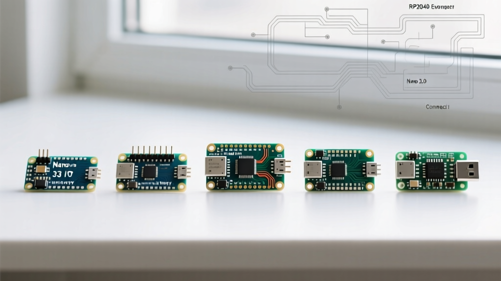
The term "Nano" no longer refers to a single ATmega328P board. Arduino has expanded the Nano footprint into a comprehensive ecosystem of specialized boards. While they share the same 18 x 45 mm mounting holes and header spacing, their component heights, power requirements, and port placements vary significantly. As noted in the guide to choosing the right Arduino board, selecting the right variant impacts both your code and your mechanical design.
| Board Variant | Core MCU | Dimensions (X-Y) | Z-Axis Max Height | USB Interface | 2026 Price Range |
|---|---|---|---|---|---|
| Nano Classic | ATmega328P | 18 x 45 mm | 4.5 mm (Mini-B) | USB Mini-B / USB-C | $20.00 - $24.00 |
| Nano Every | ATmega4809 | 18 x 45 mm | 4.2 mm (Micro-B) | USB Micro-B | $12.00 - $15.00 |
| Nano 33 IoT | SAMD21 + NINA-W10 | 18 x 45 mm | 7.5 mm (NINA Module) | USB Micro-B | $18.00 - $22.00 |
| Nano ESP32 | ESP32-S3 | 18 x 45 mm | 5.0 mm (USB-C) | USB-C | $21.00 - $25.00 |
Note: The Nano 33 IoT features the NINA-W10 Wi-Fi/Bluetooth module, which is a bulky metal shield that adds significant Z-axis height. If you are migrating a design from a Classic Nano to the 33 IoT, you must increase your enclosure's internal ceiling height by at least 3 mm to accommodate the wireless module.
The Clone Trap: Dimensional Discrepancies to Watch
The open-source nature of the original Nano design has flooded the market with $3 to $6 clones. While these are excellent for prototyping, they introduce severe mechanical inconsistencies that can ruin precision manufacturing runs.
The USB Overhang Issue
Official Arduino boards use carefully selected, recessed USB connectors that keep the total board length as close to 45.5 mm as possible. Many budget clones utilize generic through-hole USB Mini-B connectors that overhang the front edge of the PCB by an additional 2.0 mm to 3.5 mm. If you design a 3D-printed enclosure with a tight tolerance flush cutout for the USB port, a clone board simply will not fit without snapping the port off the PCB.
The 35-Mil Breadboard Spacing Anomaly
A standard 0.1" (2.54 mm or 30-mil) header pitch is universal for breadboards. However, a notorious manufacturing defect on certain batches of cheap clones shifts the outermost row of pins to a 35-mil spacing. When you attempt to plug these into a standard breadboard, the pins bind and bend. Actionable fix: If you must use bulk clones for a production run, test the first batch with digital calipers. If the 35-mil defect is present, solder female headers to the Nano and use male-to-male jumper wires, or design a custom PCB carrier that accommodates the non-standard pitch.
PCB Footprint Design Rules for Custom Carrier Boards
Integrating a Nano into a custom motherboard (rather than soldering the raw ATmega chip directly) is a common strategy for low-volume manufacturing. It allows you to flash firmware via the Nano's native USB before snapping it into your custom rig. When designing your KiCad or Altium footprint, follow these strict dimensional rules:
- Drill Sizes: Use 1.05 mm to 1.1 mm plated through-holes for the standard 0.1" male headers. This provides enough tolerance for slight variations in header pin thickness while maintaining a solid solder fillet.
- Keep-Out Zone: Maintain a strict 3 mm keep-out zone on the top layer of your carrier PCB directly beneath the Nano. The bottom of the Nano has exposed solder joints for the ICSP header and the reset button that can easily short against your carrier board's traces.
- Mounting Holes: The Nano does not have traditional corner mounting holes. It relies entirely on the friction of the 30 header pins. For high-vibration environments (like automotive or drone applications), you must design a 3D-printed clamp or add a dab of RTV silicone at the center of the board to prevent header fatigue.
Pro-Tip for PCB Designers: When downloading footprints from repositories like SnapEDA or Ultra Librarian, always verify the distance between Pin 1 (TX) and Pin 17 (A7). It must be exactly 43.18 mm (1.7 inches). Many user-submitted footprints are misaligned by a fraction of a millimeter, which will cause your silkscreen to be skewed.
Enclosure Design: USB-C vs. Legacy Ports
As the ecosystem modernizes, the transition to USB-C has altered the front-facing dimensions of the board. The Arduino Nano ESP32 and newer USB-C equipped Classic Nanos feature a port that is wider and sits slightly higher on the Z-axis than the legacy Mini-B port.
- Legacy Mini-B Cutout: 8.5 mm width x 4.0 mm height.
- Modern USB-C Cutout: 9.5 mm width x 3.8 mm height, but positioned 0.5 mm higher relative to the PCB edge.
If you are parametrically designing an enclosure in Fusion 360 or Onshape, link your USB cutout sketch to the specific board variant variable. Assuming a universal cutout will result in the USB-C cable binding against the PLA or ABS plastic, eventually cracking the enclosure wall when users forcefully insert the cable.
Frequently Asked Questions (FAQ)
What is the exact distance between the two rows of pins on an Arduino Nano?
The distance between the left and right header rows is exactly 0.6 inches (15.24 mm). This specific width is designed to perfectly bridge the center isolation trench of standard solderless breadboards, which is typically 0.3 inches wide, leaving the pins aligned with the conductive clips.
Do all Arduino Nano clones share the exact same dimensions?
No. While the PCB length and width (18x45mm) are generally respected, the Z-axis height, USB port overhang, and the placement of the voltage regulator can vary wildly between manufacturers like Elegoo, HiLetgo, and generic unbranded boards. Always measure your specific batch with calipers before finalizing injection molding or CNC-machined enclosure designs.
Can I use a Nano footprint for the Nano RP2040 Connect?
Yes, the Nano RP2040 Connect adheres to the exact same 18 x 45 mm header spacing and mounting footprint. However, like the 33 IoT, it features a dense component layout and a Wi-Fi module that increases the top-side Z-axis clearance requirement. Ensure your enclosure ceiling is at least 11 mm from the carrier board surface.
How much does an Arduino Nano weigh?
An official Arduino Nano Classic weighs approximately 5 grams (0.17 oz). The Nano ESP32 and Nano 33 IoT are slightly heavier, hovering around 6 to 7 grams due to the added mass of the RF shielding and USB-C port housing. This is a critical metric for drone and RC aircraft payload calculations.