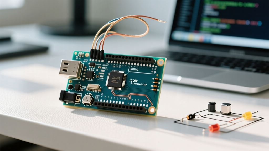

The Enduring Architecture of the Arduino Nano Board
Even in 2026, with the market saturated by high-clock-speed RP2040 and ESP32-S3 modules, the classic Arduino Nano board remains a staple on engineering workbenches. Its appeal is not raw processing power; it is the unmatched physical footprint. Measuring exactly 0.7 by 1.7 inches (18 x 43 mm) and utilizing a standard 0.6-inch (15.24 mm) DIP-30 spacing, the Nano bridges the gap between the bulk of an Uno and the surface-mount fragility of a Pro Mini. This feature deep dive bypasses the basic blink tutorials to examine the silicon realities, power delivery edge cases, and hardware traps inherent to the Nano ecosystem.
Silicon Heart: ATmega328P-AU and Clock Domains
At the core of the genuine Arduino Nano is the Microchip (formerly Atmel) ATmega328P-AU, housed in a 32-lead TQFP package. While the Uno utilizes the exact same silicon in a larger DIP-28 package, the Nano's surface-mount implementation introduces specific parasitic capacitance traits that rarely affect hobbyists but can matter in high-impedance ADC sampling. According to the Microchip ATmega328P Product Page, the chip operates with three distinct clock domains: the CPU, the I/O, and the asynchronous timer (Timer2).
The Nano drives the main system clock via a 16 MHz external quartz crystal (X1) paired with two 22pF load capacitors. This external clocking is vital for reliable UART communication. Boards attempting to run the ATmega328P on its internal 8 MHz RC oscillator often experience baud-rate drift, leading to corrupted serial data at speeds above 9600 bps.
Power Delivery and the Linear Regulator Thermal Trap
One of the most misunderstood aspects of the Arduino Nano board is its power regulation tree. The board accepts unregulated voltage on the Vin pin, which is fed into an onboard linear regulator. On genuine boards and high-quality clones, this is typically an AMS1117-5.0 in a SOT-223 package.
Thermal Math: Why 12V Can Destroy Your Nano
Many beginners assume that because the ATmega328P datasheet lists an absolute maximum rating of 6V on VCC, and the Nano documentation states a recommended Vin of 7-12V, that 12V is perfectly safe under all loads. This is a critical error. The AMS1117 SOT-223 package has a junction-to-ambient thermal resistance ($\theta_{JA}$) of roughly 60°C/W.
- Scenario A (Safe):
Vin= 9V, System Current = 50mA. Power dissipated = (9V - 5V) * 0.05A = 0.2W. Temperature rise = 12°C. - Scenario B (Thermal Shutdown):
Vin= 12V, System Current = 200mA (e.g., driving a small servo and an LCD). Power dissipated = (12V - 5V) * 0.2A = 1.4W. Temperature rise = 84°C. Add a 25°C ambient room temperature, and the regulator junction hits 109°C, triggering internal thermal protection and causing the Nano to brownout and reset continuously.
Expert Recommendation: If your project draws more than 100mA, never exceed 7.5V on the Vin pin. Better yet, bypass the linear regulator entirely by feeding a clean, regulated 5V directly into the 5V header pin.
The 3.3V Pin and Analog Pin Traps
The Nano provides a 3.3V output pin, but it is not driven by a dedicated secondary voltage regulator. Instead, it is tapped from the internal 3.3V regulator of the USB-to-Serial IC. This creates a severe current bottleneck.
CRITICAL WARNING: The 3.3V pin on a genuine Nano (using the FT232RL chip) is limited to a maximum of 50mA. On many modern clones using the CH340G, this limit drops even lower. Attempting to power an ESP8266 Wi-Fi module (which requires 170mA+ peak transmit current) from the Nano's 3.3V pin will result in immediate voltage sag, brownouts, and potential damage to the USB IC.
The A6 and A7 Digital I/O Illusion
Unlike the Arduino Uno, the Nano breaks out two extra analog pins: A6 and A7. A common point of failure in prototype code is attempting to use these as digital I/O. On the TQFP-32 ATmega328P package, ADC6 and ADC7 are physically hardwired only to the analog multiplexer. They lack digital input buffers and output latches. Calling pinMode(A6, OUTPUT) or digitalRead(A7) will compile without errors but will fail silently at runtime. You must exclusively use analogRead() for these two pins.
Comprehensive Pinout and Alternate Functions
Understanding the alternate functions of the Nano's digital pins is crucial for optimizing interrupt service routines (ISRs) and hardware communication protocols. Below is the definitive mapping for the ATmega328P on the Nano footprint.
| Pin | Primary Function | Alternate / Hardware Functions | Notes & Edge Cases |
|---|---|---|---|
| D0 (RX) | Digital I/O | UART RX, PCINT19 | Shares line with USB IC. Pulls high via 1k resistor. |
| D1 (TX) | Digital I/O | UART TX, PCINT20 | Shares line with USB IC. LED on some clones. |
| D2 | Digital I/O | INT0 (External Interrupt) | Hardware interrupt 0. Critical for encoders. |
| D3 | Digital I/O | INT1, OC2B (PWM) | Hardware interrupt 1. 8-bit PWM via Timer2. |
| D10 | Digital I/O | SS (SPI), OC1B (PWM) | Must be set as OUTPUT for SPI Master mode. |
| D11 | Digital I/O | MOSI (SPI), OC2A (PWM) | Hardware SPI data out. |
| D12 | Digital I/O | MISO (SPI) | Hardware SPI data in. No PWM capability. |
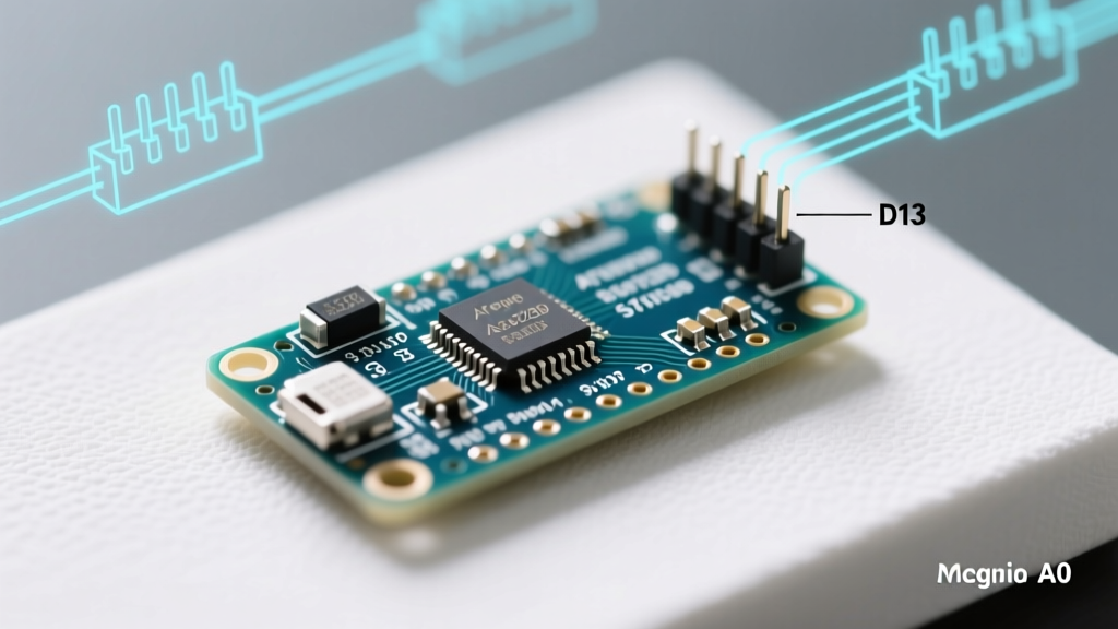
| D13 | Digital I/O | SCK (SPI), Onboard LED | Flashes on boot via bootloader. SPI Clock. |
| A4 | Analog In | SDA (I2C), PCINT12 | Hardware I2C Data. Has internal pull-up. |
| A5 | Analog In | SCL (I2C), PCINT13 | Hardware I2C Clock. Has internal pull-up. |
| A6 / A7 | Analog In ONLY | ADC6 / ADC7 | No digital I/O. No internal pull-ups. |
USB-to-Serial ICs: FT232RL vs. the CH340 Clone Ecosystem
The official Arduino Nano Official Documentation specifies the FTDI FT232RL as the USB-to-UART bridge. However, the 2026 market is dominated by clone boards utilizing the WCH CH340G or CH340C chips due to aggressive supply chain pricing. For driver installation and troubleshooting on these clone variants, the SparkFun CH340 Driver Installation Guide remains the definitive resource.
CH340G vs CH340C: If you are designing a custom PCB based on the Nano schematic, opt for the CH340C. Unlike the CH340G, the 'C' variant includes an integrated clock oscillator, eliminating the need for an external 12MHz crystal and two load capacitors, thereby saving board space and reducing BOM costs.
Bootloader Fragmentation and ISP Recovery
A persistent headache when programming the Arduino Nano board via the IDE is the "Programmer is not responding" or "avrdude: stk500_recv(): programmer is not responding" error. This is almost always tied to bootloader fragmentation.
- The Old Bootloader (ATmegaBOOT): Pre-2018 genuine Nanos and the vast majority of cheap clones ship with the legacy ATmegaBOOT. It occupies 2KB of flash memory and communicates at a sluggish 19200 baud.
- The New Bootloader (Optiboot): Modern genuine Nanos ship with Optiboot. It uses only 512 bytes of flash (freeing up 1.5KB for your code) and communicates at 115200 baud.
The Fix: If your upload fails, first change the IDE Tools menu to "ATmega328P (Old Bootloader)". If you want to permanently modernize a clone board, connect an external USBasp ISP programmer to the ICSP header (pins MISO, MOSI, SCK, Reset, 5V, GND) and select "Burn Bootloader" in the IDE. This flashes the Optiboot bootloader and permanently sets the board's fuses to expect a 115200 baud serial handshake.
Real-World Failure Modes: The Backfeed Diode Omission
When designing enclosures that require both USB debugging and external battery power, engineers must be aware of a dangerous hardware omission on clone Nano boards. The genuine Nano schematic includes a Schottky diode (typically a 1N5819 or similar) between the USB VBUS (5V) and the board's main +5V net. This prevents external power applied to the 5V pin from backfeeding into your computer's USB port.
Many budget clones omit this diode to save fractions of a cent. If you plug a 5V battery pack into the 5V and GND pins while the USB cable is connected to your PC, the battery voltage will fight the PC's USB power supply. This can trip your motherboard's overcurrent protection, shut down the PC's USB hub, or permanently fry the FT232/CH340 chip. Always unplug the USB before injecting 5V directly into the Nano's header pins on clone boards.
Summary: Maximizing the Nano's Potential
The Arduino Nano board is a masterclass in pragmatic engineering. By respecting the thermal limits of the onboard linear regulator, acknowledging the analog-only nature of A6 and A7, and managing the bootloader and backfeed quirks of the clone market, you can deploy the Nano in robust, long-term embedded applications. It remains an indispensable platform for rapid prototyping and space-constrained DIY electronics in 2026 and beyond.