
The Core Definition: Understanding Electrostatic Charge
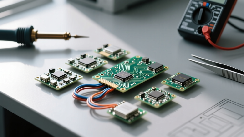
When you shuffle your feet across a carpeted room and reach for a metal doorknob, you experience a fundamental principle of physics in real-time. In electrical engineering and physics, the buildup of electric charges on an object is called static electricity, or more formally, an electrostatic charge. For electronics hobbyists, electricians, and PCB designers, this phenomenon is not just a minor shock hazard; it is the root cause of Electrostatic Discharge (ESD), a silent killer of modern microcontrollers, MOSFETs, and integrated circuits.
As you progress along the skill-building path in electronics, transitioning from soldering basic through-hole resistors to programming bare-metal ARM Cortex microcontrollers or handling bare die RF components, mastering ESD mitigation becomes non-negotiable. A spark you cannot even feel occurs at roughly 3,000 volts. However, modern nanometer-scale silicon can be permanently destroyed by an ESD event as low as 20 volts. This guide outlines a structured, four-phase skill path to understanding, measuring, and neutralizing static charge in your workspace.
Skill Phase 1: Mastering the Triboelectric Series
The first step in ESD defense is understanding how the buildup occurs. The triboelectric effect is the primary mechanism where materials gain or lose electrons through friction and separation. To build your foundational knowledge, you must know where common bench materials sit on the triboelectric series.
| Material (Positive / Electron Donor) | Material (Negative / Electron Acceptor) | Typical Voltage Generated (Low Humidity) |
|---|---|---|
| Human Hands / Hair | Nylon / Wool | 10,000V - 35,000V (Walking on carpet) |
| Glass / Quartz | Polyurethane / PVC | 5,000V - 15,000V (Peeling tape) |
| Cotton / Paper | Polyester / Kapton Tape | 2,000V - 8,000V (Sliding plastic bins) |
| Steel / Copper (Grounded) | Silicone / Teflon | 1,000V - 4,000V (Soldering iron wipes) |
Expert Insight: Notice that Kapton tape (polyimide), heavily used in electronics for high-temp masking, is highly electronegative. Peeling Kapton tape off a PCB in a dry environment can generate localized surface voltages exceeding 10kV, easily inducing a catastrophic field-induced ESD event on nearby exposed traces.
Skill Phase 2: Component Vulnerability Mapping
Not all components react to the buildup of electric charges equally. As you advance your diagnostic skills, you must learn to identify which parts of your bill of materials (BOM) require strict ESD protocols.
The Human Body Model (HBM) vs. Charged Device Model (CDM)
The EOS/ESD Association classifies ESD events into distinct models. The Human Body Model (HBM) simulates a person discharging into a component, modeled as a 100 pF capacitor discharging through a 1.5 kΩ resistor. The Charged Device Model (CDM) simulates a component itself becoming charged (e.g., sliding down a plastic feeder tube) and discharging into a grounded PCB pad. CDM events have vastly faster rise times (<1 nanosecond) and higher peak currents, making them exceptionally lethal to modern ICs.
| Component Class | Examples | Typical HBM Failure Threshold | Vulnerability Notes |
|---|---|---|---|
| Discrete Passives | 0805 Resistors, MLCC Capacitors | > 4,000V | Highly robust; rarely fail from standard handling. |
| Bipolar Junction Transistors | 2N3904, TIP31C | 2,000V - 5,000V | Moderate tolerance; junction breakdown requires high energy. |
| Operational Amplifiers | LM358, NE5532 | 1,000V - 2,500V | Input stage gate oxides can degrade, causing offset drift. |
| Power MOSFETs | IRF540N, IRLZ44N | 100V - 500V | Gate oxide is extremely thin. A 50V spike causes a short. |
| Advanced MCUs / FPGAs | STM32, Xilinx Artix-7 | 50V - 250V (CDM) | Nanometer nodes have microscopic dielectric layers. Highly sensitive. |
Skill Phase 3: Architecting the ESD-Safe Bench
Moving from theory to practical application requires building a properly grounded workstation. A common beginner mistake is simply strapping a piece of copper to a desk and wiring it directly to the earth pin of a wall outlet. This is dangerous and ineffective. According to Analog Devices' ESD guidelines, an ESD-safe bench relies on controlled dissipation, not dead-short grounding.
The 1 Megohm Safety Rule
Every connection to ground in an ESD workspace—whether it is your wrist strap, your bench mat, or your floor mat—must pass through a 1 megohm (1MΩ) resistor.
- Safety: If you accidentally touch a live 120V/240V AC mains wire while wearing a grounded wrist strap, the 1MΩ resistor limits the current through your heart to a non-lethal fraction of a milliamp.
- Physics: Static charge dissipates effectively through 1MΩ. The RC time constant of a human body (approx. 150 pF) discharging through 1MΩ is roughly 150 microseconds. This bleeds off dangerous static voltages long before you can touch a sensitive IC, without creating a rapid discharge that could induce an electromagnetic pulse (EMP) on the bench.
Selecting the Right Mat Materials
When buying a bench mat (such as the Desco Statfree series or 3M static dissipative mats), you must understand surface resistivity:
- Conductive (< 10^5 Ω/sq): Bleeds charge instantly. Too fast for sensitive bare ICs; can cause CDM-style rapid discharge damage.
- Static Dissipative (10^5 to 10^9 Ω/sq): The gold standard for electronics workbenches. Safely bleeds charge at a controlled rate.
- Insulative (> 10^9 Ω/sq): Standard plastics, wood, and rubber. These trap the buildup of electric charges and must be removed from the bench.
Skill Phase 4: Advanced Measurement & Forensics
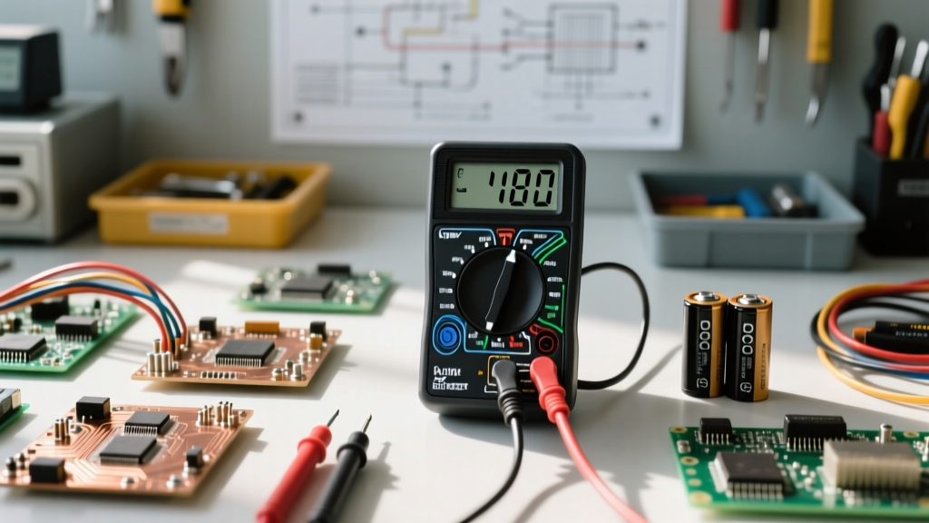
The final stage of the skill-building path is learning to measure and visualize electrostatic events. Because ESD happens in nanoseconds, standard digital multimeters are entirely useless for capturing an ESD strike.
Capturing ESD with an Oscilloscope
To truly understand the buildup and discharge of electric charges, advanced technicians use oscilloscopes equipped with high-bandwidth probes or Near-Field Magnetic Sniffers (like the Langer EMV RF-R series). By looping a small coaxial sniffer probe over an ungrounded PCB trace and triggering the oscilloscope on a high-frequency edge, you can capture the electromagnetic interference (EMI) signature of an ESD event occurring nearby.
Per the IEC 61000-4-2 standard, a typical contact ESD discharge features a rise time of less than 1 nanosecond (0.8ns) and a secondary decay phase lasting around 60 nanoseconds. If your oscilloscope lacks a 1 GHz+ bandwidth, you will not capture the initial destructive spike, leading to a false sense of security when debugging a failing prototype.
Using Electrostatic Field Meters
For non-contact verification of your workspace, invest in an electrostatic field meter (such as the Trek Model 511 or a budget-friendly UNI-T UT334). These devices measure the electric field gradient in kilovolts per meter (kV/m). By scanning your workbench, plastic component bins, and even your clothing, you can identify hidden insulators that are hoarding static charge before they have the chance to arc into your expensive prototype boards.
Summary of the ESD Skill Path
Recognizing that the buildup of electric charges on an object is called static electricity is merely the starting line. True proficiency in electronics requires a holistic approach: respecting the triboelectric nature of your materials, understanding the nanometer-scale vulnerabilities of modern silicon, engineering a dissipative (not just conductive) workspace, and utilizing high-bandwidth forensic tools to verify your environment. By mastering these four phases, you transition from a hobbyist who occasionally fries components to a reliable engineer capable of handling aerospace-grade, ESD-sensitive hardware with absolute confidence.