
The Metallurgical Paradox: Why Gold in Electronics?
A common misconception among electronics beginners and amateur scrappers is that gold (Au) is used in circuitry because it is the best electrical conductor. In reality, silver (63.0 × 10⁶ S/m) and copper (59.6 × 10⁶ S/m) both boast higher bulk conductivity than gold (45.2 × 10⁶ S/m). The true reason electronic components with gold are ubiquitous in high-reliability systems is gold's absolute nobility.
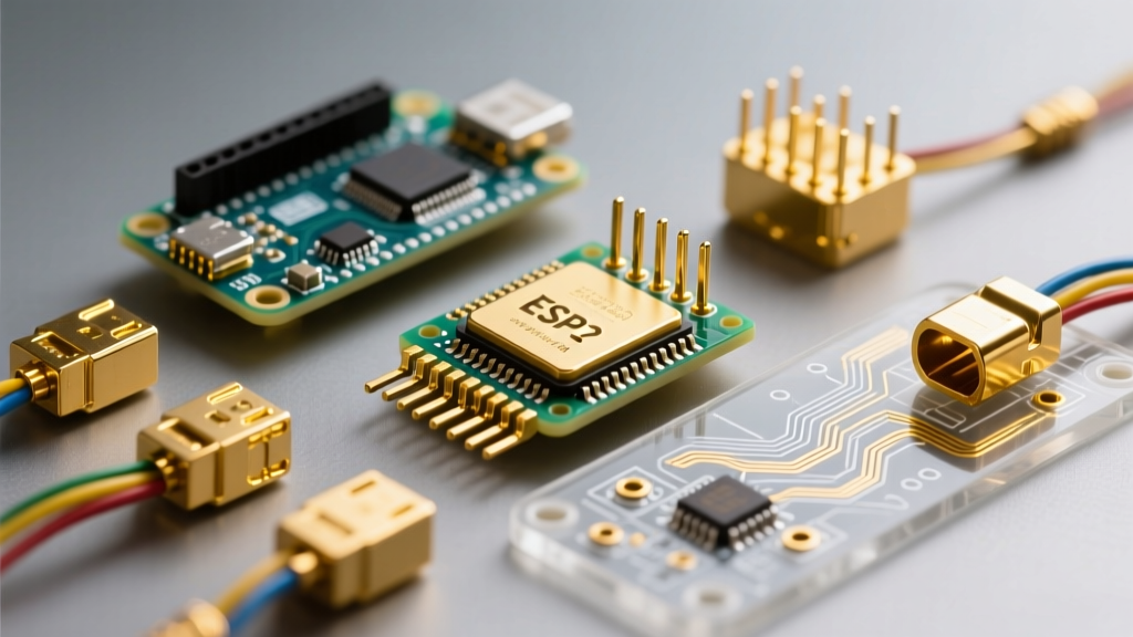
Unlike silver, which forms a resistive tarnish (silver sulfide), or copper, which rapidly oxidizes into a non-conductive green patina, gold does not react with oxygen or moisture. In low-voltage, low-current digital logic circuits (such as 3.3V or 5V microcontroller I/O), even a microscopic layer of oxidation on a copper contact can introduce enough resistance to cause signal failure. Gold guarantees near-zero contact resistance over decades of operation, making it indispensable for edge connectors, switch contacts, and IC packaging.
Mapping Gold in Electronic Components
Not all gold-bearing e-waste is created equal. The thickness of the gold layer, the underlying substrate, and the alloy composition dictate both the component's function and its recovery value. Below is a structural breakdown of where gold is typically found in modern and legacy electronics.
| Component Type | Gold Application | Typical Thickness | Scrap / Recovery Tier |
|---|---|---|---|
| RAM / PCIe Edge Fingers | Hard Gold Plating (Cobalt alloyed) | 30–50 µin (0.7–1.2 µm) | Tier 1 (High Yield) |
| Vintage Ceramic CPUs | Gold-plated pins & heat spreaders | Variable (Heavy flash) | Tier 1 (High Yield) |
| Telecom Backplanes | Hard Gold / ENIG routing | 20–40 µin | Tier 1 (High Yield) |
| Standard IC Pins (DIP/SOP) | Gold Flash / Matte Tin | 2–5 µin (0.05–0.12 µm) | Tier 2 (Medium Yield) |
| Modern CPUs (FC-BGA) | ENIG Substrate / Internal wires | Trace (< 2 µin surface) | Tier 3 (Low Yield) |
| Reed Switches / Relays | Solid Gold/Ruthenium Alloy | Solid Mass | Tier 1 (High Yield) |
PCB Surface Finishes: ENIG vs. Hard Gold
When examining printed circuit boards (PCBs), identifying the type of gold finish is critical for determining recovery potential. The industry primarily relies on two distinct gold-based surface finishes:
1. Electroless Nickel Immersion Gold (ENIG)
ENIG is the standard for modern surface-mount technology (SMT) pads. It consists of a copper pad, a layer of electroless nickel (typically 120–240 µin), and a very thin immersion gold layer (1–3 µin). The gold exists solely to protect the underlying nickel from oxidation during storage and soldering. Once the board is soldered, the gold dissolves into the solder joint, forming a brittle gold-tin intermetallic compound. From a recovery standpoint, ENIG boards yield very little gold per pound, often making the chemical processing cost-prohibitive for hobbyists.
2. Electroplated Hard Gold
Used almost exclusively on edge connectors (like DDR4/DDR5 RAM fingers) and switch contacts, hard gold is alloyed with cobalt or nickel to increase wear resistance. It is plated to a much thicker specification (30–50 µin) to withstand thousands of insertion cycles. This is the primary target for e-waste recyclers, as the gold layer is thick enough to yield measurable returns when chemically stripped or mechanically separated.
The Generational Shift: Vintage vs. Modern Silicon
A crucial concept in urban mining is the architectural shift in microprocessors. Scrappers who target modern processors often face disappointing yields due to the transition from Pin Grid Array (PGA) to Flip-Chip Ball Grid Array (FC-BGA).
- Vintage Ceramic CPUs (Pre-2005): Processors like the Intel Pentium Pro, AMD K6, and early Motorola 68k series featured heavy gold-plated pins and gold-plated ceramic lids. A single pound of these ceramic CPUs can yield several grams of pure gold.
- Modern FC-BGA CPUs (2010–Present): Modern Intel Core and AMD Ryzen processors use solder balls (primarily Tin/Silver/Copper) for motherboard interconnection. The gold is relegated to microscopic bonding wires inside the epoxy package or trace amounts in the substrate's ENIG finish. Processing modern CPUs for gold is largely unprofitable at the hobbyist scale due to the overwhelming volume of fiberglass, epoxy, and copper that must be dissolved to reach trace gold amounts.
Assaying and Identification Techniques
Visually identifying gold is unreliable; many modern connectors use yellow-colored tin-zinc alloys or thin gold flashes over nickel that mimic heavy plating. Professionals rely on precise analytical tools.
X-Ray Fluorescence (XRF) Spectrometry
Handheld XRF analyzers, such as the Thermo Fisher Niton XL2 or Olympus Vanta L, are the industry standard for non-destructive precious metal assaying. These devices fire X-rays into the sample and measure the fluorescent energy signature to determine exact elemental composition and plating thickness. However, with 2026 market prices ranging from $18,000 to $35,000 per unit, XRF is strictly a commercial tool.
The Scratch and Acid Test (Hobbyist Method)
For hobbyists, testing edge connectors requires a destructive approach. Using a jeweler's file to cut through the surface layer, followed by a drop of nitric acid (HNO3), will reveal the truth. If the filed area turns green, the underlying metal is copper or brass, and the surface was merely gold flash. If the filed area remains unaffected and only the surface gold dissolves, it indicates a thicker hard gold plating over nickel.
Chemical Recovery: Realities and Protocols
Recovering gold from electronic components is a hazardous chemical engineering process, not a simple weekend craft. The most common method for dissolving gold is Aqua Regia (Royal Water), a highly corrosive mixture of one part concentrated nitric acid and three parts concentrated hydrochloric acid.
⚠️ CRITICAL SAFETY WARNING: Aqua Regia generates nitrogen dioxide (NO2) and chlorine (Cl2) gases during the dissolution process. These gases are highly toxic and potentially lethal. Refining must only be performed inside a certified, chemically resistant fume hood with proper scrubbing systems. Never attempt Aqua Regia refining in a residential garage or unventilated space.
The Precipitation Workflow
- Dissolution: Gold-bearing components (pre-stripped of base metals like copper and aluminum using sulfuric or hydrochloric acid) are submerged in Aqua Regia. The gold oxidizes and enters the solution as chloroauric acid (HAuCl4).
- Filtration: The solution is filtered to remove insoluble silver chloride (AgCl) and other particulate debris.
- Neutralization: Excess nitric acid must be destroyed before precipitation. This is typically achieved by adding Urea or by boiling the solution down to a syrup and reconstituting it with distilled water and HCl.
- Precipitation: A reducing agent, most commonly Sodium Metabisulfite (SMB), is added to the chloroauric acid solution. The SMB reduces the gold ions back into solid, elemental gold powder, which drops to the bottom of the beaker as a brown mud.
- Smelting: The dried gold powder is mixed with a flux (such as borax and sodium carbonate) and melted in a crucible using an oxy-acetylene torch or induction furnace at 1,064°C (1,947°F) to form a pure 24k gold button.
The Economics of Urban Mining
The financial viability of scrapping electronic components with gold depends entirely on volume and grade. According to data from the Global E-waste Statistics Partnership (GESP), the concentration of precious metals in certain e-waste streams vastly exceeds that of natural ores. While a high-grade underground gold mine might yield 5 to 10 grams of gold per metric ton of ore, a metric ton of high-grade telecom backplanes or legacy RAM fingers can yield between 300 and 800 grams of gold.
However, the United States Environmental Protection Agency (EPA) emphasizes that improper handling of e-waste releases severe environmental toxins, including lead, beryllium, and brominated flame retardants. Professional recyclers offset the high costs of environmental compliance and chemical disposal through the simultaneous recovery of copper, palladium, and silver, which often constitute a larger percentage of the board's total scrap value than the gold itself. For the individual DIYer, the most profitable and safe approach is to mechanically harvest and sort high-grade gold fingers and ceramic CPUs, selling them directly to specialized precious metal refiners rather than attempting in-house chemical recovery.
Summary of Best Practices for Hobbyists
- Sort by Grade: Keep telecom boards, RAM, and ceramic CPUs separate from standard consumer motherboards.
- Avoid Modern CPUs: Do not waste chemical reagents on post-2010 FC-BGA processors; their gold content is negligible.
- Harvest Mechanically: Use specialized edge-connector cutters or shears to remove gold fingers from PCBs before selling or refining, leaving the worthless fiberglass behind.
- Respect the Chemistry: If refining, invest in proper PPE (respirators, heavy nitrile gloves) and a functional fume hood before purchasing a single liter of acid.
Understanding the exact metallurgical purpose and physical location of gold in electronics transforms scrapping from a game of chance into a calculated, profitable science. By focusing on hard-gold applications and legacy architectures, enthusiasts can maximize their yields while minimizing chemical waste.