
Introduction to AGC Materials in Modern Manufacturing
As the semiconductor and RF industries push toward 6G communications and advanced AI packaging in 2026, the materials used at the substrate level have become increasingly complex. AGC Inc.'s electronic components business products are at the forefront of this evolution, supplying critical multilayer ceramic packages, glass core substrates, and low-loss fluoropolymer laminates. However, the very properties that make these materials exceptional—such as ultra-low dielectric constants and precise coefficients of thermal expansion (CTE)—also make them highly sensitive to improper handling.
For lab technicians, manufacturing engineers, and procurement specialists, treating AGC components like standard FR-4 printed circuit boards is a recipe for catastrophic failure. A single micro-fracture in a glass core substrate or an electrostatic discharge (ESD) event on a bare ceramic package can result in thousands of dollars in scrapped materials and delayed production timelines. This guide outlines the strict safety, handling, and integration best practices required for AGC's specialized electronic product lines.
Hazard Matrix: AGC Product Lines and Failure Modes
Before establishing handling protocols, it is crucial to understand the specific physical and electrical vulnerabilities of AGC's primary product categories. The table below maps material types to their most common failure modes in a manufacturing environment.
| Product Category | Primary Application | Mechanical Hazard | Thermal / ESD Hazard |
|---|---|---|---|
| Glass Core Substrates | 2.5D/3D IC Packaging, AI Accelerators | Edge chipping, micro-cracking from vacuum wand misuse | Static attraction of particulates; localized thermal shock |
| Multilayer Ceramic Packages | GaN/SiC High-Power RF Amplifiers | Brittle fracture under uneven mounting torque | CTE mismatch during reflow; pad cratering |
| Low-Loss Fluoropolymer Laminates | 5G/6G mmWave Antennas, Radar | Delamination from improper mechanical prep | Dielectric breakdown via ESD; thermal degradation >280°C |
ESD and Micro-Contamination Protocols for Glass Substrates
AGC’s glass core substrates are revolutionizing high-density interconnects due to their superior dimensional stability compared to organic substrates. However, glass is an inherent insulator. In a dry cleanroom environment (often kept at 40% relative humidity or lower), glass substrates can easily accumulate static charges exceeding 2,000V simply from friction during transport.
The Particulate Attraction Risk
While the glass itself may not suffer immediate dielectric breakdown from a 2kV charge, the electrostatic field will aggressively attract micro-particulates from the air. If these particulates settle inside the Through Glass Vias (TGVs) prior to copper plating, it causes voids and open circuits. According to the ESD Association's fundamentals on insulators, standard grounding wrist straps do not dissipate charges on insulative materials like glass.
- Best Practice: Always handle AGC glass substrates using ionized air blowers or ionizing bars calibrated to neutralize charges within 1.5 seconds.
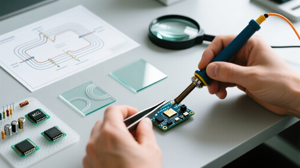
- Tooling: Use ESD-safe, soft-tipped vacuum wands (e.g., PEEK or Delrin tips with a Shore A hardness below 60) to prevent edge chipping. Never use rigid metal tweezers on the substrate edges.
- Cost of Failure: Scratching or contaminating a single 300mm glass core substrate can result in upwards of $4,500 in lost fab time and ruined downstream lithography processes.
Thermal Shock Prevention in Ceramic Packages
AGC’s multilayer ceramic packages (often utilizing Alumina or Aluminum Nitride bases) are designed to pull heat away from high-power GaN and SiC dies. The primary safety and reliability concern during PCB assembly is the Coefficient of Thermal Expansion (CTE) mismatch.
Calculating Safe Ramp Rates
Ceramic packages typically exhibit a CTE of 6.5 to 7.5 ppm/°C, which closely matches silicon but clashes heavily with standard FR-4 PCBs (14–17 ppm/°C). During the reflow soldering process, the cooling phase is the most dangerous. If the cooling ramp rate is too aggressive, the shear stress at the solder joint interface will exceed the tensile strength of the ceramic, causing micro-fractures or pad cratering.
Critical Warning: Never force-cool AGC ceramic packages using compressed air or liquid nitrogen immediately after reflow. The cooling ramp rate must be strictly limited to < 3°C per second to prevent catastrophic brittle fracture.
Furthermore, when mounting heavy ceramic packages to heatsinks, mechanical torque must be perfectly distributed. For standard M3 mounting screws on AGC ceramic flanges, the maximum recommended torque is 0.4 N·m. Always use a calibrated torque screwdriver and a star-pattern tightening sequence to avoid inducing localized stress fractures.
Chemical Compatibility and Moisture Sensitivity
While ceramics and glass are generally impervious to moisture, the packaging and specific laminate structures require strict environmental controls.
Fluoropolymer Laminates and Chemical Exposure
AGC’s low-loss laminates (such as their proprietary fluoropolymer-based materials) are highly sensitive to certain aggressive fluxes and cleaning solvents. Using standard alkaline saponifiers in an inline PCB washer can degrade the resin matrix, leading to delamination and an increase in the dissipation factor (Df), which ruins mmWave signal integrity.
- Cleaning Protocol: Use only neutral pH (6.5 - 7.5) aqueous cleaners specifically validated for fluoropolymer and PTFE-based laminates.
- Flux Selection: Opt for no-clean, low-residue fluxes. If cleaning is mandatory, verify the solvent's compatibility with AGC's specific datasheet for the laminate series being used.
Moisture Sensitivity Levels (MSL) in Ceramics
It is a common misconception that ceramic packages are immune to moisture damage. While the ceramic body won't absorb water, the internal brazing materials, unglazed via edges, and attached die-attach films can trap moisture. If subjected to 260°C lead-free reflow temperatures, this trapped moisture vaporizes, causing internal delamination (the "popcorn effect").
Follow IPC/JEDEC J-STD-033 standards for handling moisture-sensitive devices. If AGC ceramic components have been exposed to ambient factory conditions (30°C/60% RH) beyond their specified floor life, they must be baked at 125°C for 24 hours in a nitrogen-purged oven before reflow.
Procurement Safety: Avoiding the Gray Market
Safety and best practices extend beyond the lab and into the supply chain. In 2026, the global shortage of advanced semiconductor packaging materials has led to a surge in gray-market counterfeit components. Counterfeit AGC ceramic packages or glass substrates often utilize inferior, high-alkali glass or low-purity alumina.
The Danger of High-Alkali Glass: Inferior glass contains high levels of sodium and potassium ions. Under high voltage and elevated temperatures, these ions migrate through the dielectric, creating conductive dendrites that eventually cause a dead short. This failure mode often passes initial QA testing but manifests as a field failure after 500 to 1,000 hours of operation.
- Verification: Always procure AGC electronic components business products through authorized, franchised distributors.
- Traceability: Demand full lot traceability and Certificates of Compliance (CoC) directly from AGC or their tier-1 authorized partners.
- Visual Inspection: Inspect incoming ceramic packages under a 40x microscope. Genuine AGC ceramics feature highly uniform grain structures and precise, laser-etched lot codes. Counterfeits often show porous edges and inconsistent metallization thickness on the braze rings.
Summary of Best Practices
Integrating AGC’s advanced materials into next-generation electronics requires a paradigm shift from traditional PCB handling. By enforcing strict ionization protocols for glass substrates, limiting thermal ramp rates to under 3°C/sec for ceramics, and maintaining rigorous supply chain traceability, engineering teams can fully leverage the performance benefits of AGC products while mitigating the risk of costly manufacturing defects.