
Decoding the Potentiometer Schematic Diagram Symbols
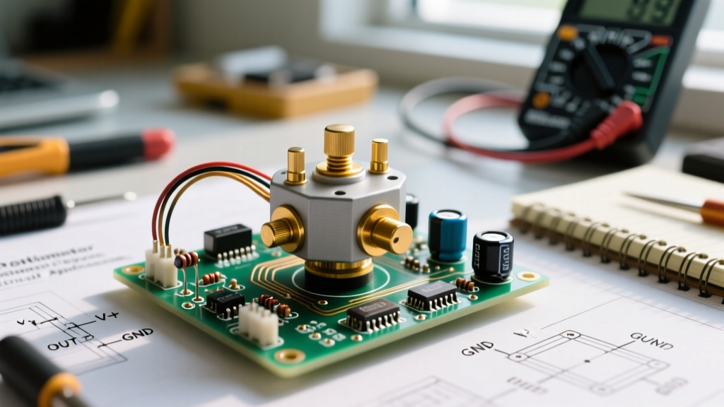
When designing analog control interfaces, audio mixing consoles, or precision sensor calibration circuits, the potentiometer schematic diagram is your foundational blueprint. Unlike a simple fixed resistor, a potentiometer (or 'pot') is a three-terminal electromechanical device that introduces dynamic variability into a circuit. However, reading and drawing the schematic for a pot requires understanding not just the symbol, but the functional intent behind how the three pins—Terminal 1, Terminal 2 (the wiper), and Terminal 3—are deployed.
IEEE vs. IEC Standard Representations
In North America, the IEEE standard represents a potentiometer using a zig-zag resistor symbol with an arrow pointing at the center, denoting the wiper. In European and international designs, the IEC standard uses a rectangular box with the same wiper arrow. In both cases, the arrow is the critical element: it signifies the mechanical or digital linkage that sweeps across the resistive track, dividing the total resistance into two variable, complementary segments.
Core Circuit Applications: 3-Terminal vs. 2-Terminal Wiring
A common mistake among novice prototypers is assuming that a potentiometer schematic diagram must always utilize all three terminals. In reality, the schematic changes drastically depending on whether the component is acting as a voltage divider or a variable resistor.
Configuration A: The Voltage Divider (3-Terminal)
The most common application of a potentiometer is as a voltage divider. In this schematic configuration, the input voltage ($V_{in}$) is applied across Terminal 1 and Terminal 3, while the output voltage ($V_{out}$) is read from the wiper (Terminal 2). As detailed in SparkFun's guide to voltage dividers, the output is calculated using the ratio of the resistances on either side of the wiper.
If you have a 10kΩ linear potentiometer connected to a 5V reference, and the wiper is positioned at 30% of the physical travel, the resistance between Terminal 1 and the wiper is 3kΩ, and between the wiper and Terminal 3 is 7kΩ. The schematic math dictates an output of exactly 1.5V. This configuration is ubiquitous in microcontroller ADC inputs, reference voltage generation, and joystick positioning.
Configuration B: The Rheostat / Variable Resistor (2-Terminal)
When a schematic requires variable current limiting—such as adjusting the bias current of a transistor or dimming a high-power LED—the potentiometer is wired as a rheostat. The schematic will show the wiper connected to only one end terminal.
Expert Engineering Tip: Never leave the third terminal floating in a rheostat configuration. A robust potentiometer schematic diagram will always show a jumper wire tying the wiper to the unused terminal. If mechanical vibration or track oxidation causes the wiper to momentarily lose contact, a floating terminal results in an open circuit (infinite resistance), which can destroy sensitive downstream components. Tying it off caps the maximum resistance at the pot's rated value, ensuring fail-safe operation.
Component Selection: Audio Taper vs. Linear Taper in Schematics
While the schematic symbol for a linear taper (B-taper) and a logarithmic/audio taper (A-taper) looks identical, the functional behavior is vastly different. Human hearing perceives loudness logarithmically. If you use a linear 100kΩ potentiometer for an audio volume control, 80% of the perceived volume change will happen in the first 20% of the knob's rotation, making precise adjustments impossible.
When drafting a schematic for an audio preamplifier or guitar pedal, you must specify an 'A-taper' potentiometer in the Bill of Materials (BOM), even if the schematic symbol remains standard. For deeper insights into electromechanical component behaviors, All About Circuits provides an excellent breakdown of taper curves and their specific use cases.
Real-World Troubleshooting: Wiper Noise and Load Impedance
A schematic diagram represents an ideal world, but physical potentiometers introduce parasitic elements. Two major failure modes frequently plague prototyped circuits:
- Wiper Noise (Crackling): Common in cheap carbon-track potentiometers. As the wiper moves, microscopic carbon dust and oxidation create transient resistance spikes. In audio circuits, this manifests as loud crackling. Upgrading to conductive plastic or cermet track potentiometers resolves this.
- Loading Effects: If your potentiometer schematic diagram feeds a wiper directly into a low-impedance load (e.g., a 1kΩ resistor or an unbuffered audio amplifier), the voltage divider math breaks down. The load impedance acts in parallel with the lower half of the potentiometer, causing severe non-linearity and signal droop.
Component Matrix: Selecting the Right Potentiometer
Choosing the correct physical component to match your schematic requirements is critical for long-term reliability. Below is a comparison of industry-standard models based on track material and application.
| Model Series | Track Material | Standard Taper | Ideal Schematic Application |
|---|---|---|---|
| Bourns 3296W (Trimpot) | Cermet | Linear (B) | PCB-mounted calibration, sensor zeroing, one-time factory adjustments. |
| Alpha RD901F | Carbon | Audio (A) | Panel-mount audio mixers, guitar amplifier volume controls. |
| TT Electronics P160 | Conductive Plastic | Linear (B) | High-cycle precision servos, medical equipment, low-noise joysticks. |
For rigorous environmental specifications and lifecycle ratings of cermet trimpots, refer to the official Bourns 3296 datasheet, which outlines the exact rotational life and contact resistance variations you must account for in precision schematics.
Advanced Implementation: Buffering the Wiper Output
To eliminate the loading effects mentioned earlier, professional schematics incorporate an active buffer. When a 100kΩ potentiometer is set to the 50% mark, its Thevenin equivalent output impedance is 25kΩ. If this drives a microcontroller ADC with a sample-and-hold capacitor, the high impedance will cause reading inaccuracies and extended settling times.
Preventing Loading Effects with Op-Amps
The solution is to add a unity-gain buffer amplifier to the schematic. By routing the wiper into the non-inverting input (+) of an operational amplifier (such as the TL072 for audio or the LM358 for general DC applications) and tying the output directly to the inverting input (-), you achieve an ideal voltage follower. The op-amp presents an input impedance in the gigaohm range, drawing virtually zero current from the potentiometer wiper, while providing a low-impedance output capable of driving heavy loads, long cables, or low-resistance ADC networks without signal degradation.
Mastering the potentiometer schematic diagram is about bridging the gap between theoretical symbols and physical realities. By specifying the correct taper, implementing fail-safe rheostat tie-offs, and buffering high-impedance wiper outputs, you ensure your analog circuits perform flawlessly in the real world.