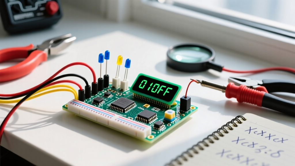
The optimal breadboard-friendly audio amplifier circuit for DIY bench work is a discrete Class AB push-pull topology. Specifically, use a 2N3904 voltage amplifier stage (VAS) driving a TIP31C (NPN) and TIP32C (PNP) complementary output pair, biased by two 1N4148 diodes, powered by a ±12V dual supply. This configuration delivers roughly 5W RMS into an 8Ω load with less than 1% THD, avoiding the thermal waste of Class A and the crossover distortion of Class B.
The Discrete Class AB Audio Amplifier Circuit Topology
To understand why this topology wins for general-purpose audio, we must look at the alternatives. A Class B amplifier uses a push-pull pair with zero quiescent bias, resulting in a dead zone where neither transistor conducts as the signal crosses 0V. This creates harsh crossover distortion. A Class A amplifier biases the output transistor fully on at all times, eliminating distortion but capping efficiency at 25%—meaning a 5W audio output requires dissipating 15W+ of heat.
The Class AB topology solves both by injecting a small quiescent bias current (typically 20mA to 50mA) through the output transistors. This keeps both devices just barely turned on at the zero-crossing, eliminating the dead zone while maintaining 50-60% efficiency.
Node Labels and Signal Path
Our circuit relies on five critical nodes to manage the signal and DC bias:
- Node A (Input / VAS Base): Receives the AC audio signal via a coupling capacitor and the DC negative feedback from the output.
- Node B (VAS Collector / NPN Drive): The high-impedance gain node. Drives the base of the NPN output transistor.
- Node C (PNP Base Drive): Separated from Node B by the bias diodes. Drives the base of the PNP output transistor.
- Node D (Bias Midpoint): The junction between the two bias diodes. Sits exactly 0.6V below Node B and 0.6V above Node C.
- Node E (Output / Emitter Junction): Where the emitter resistors of the push-pull pair meet. Connects to the speaker load and the global feedback loop.
Design Walkthrough: Selecting Real Component Values
Let's assign exact part numbers and values for a ±12V dual-rail supply targeting an 8Ω speaker load. According to Electronics Tutorials on Class AB Amplifiers, thermal stability in the output stage is critical, requiring emitter degeneration resistors.
- Q1 (VAS): 2N3904 (NPN small-signal)
- Q2 (NPN Output): TIP31C (NPN power, 100V Vceo, 3A Ic)
- Q3 (PNP Output): TIP32C (PNP power, 100V Vceo, 3A Ic)
- D1, D2 (Bias): 1N4148 (small-signal switching diodes)
- R_bias: 2.2kΩ, 1/4W (from +12V to Node B)
- R_e1, R_e2: 0.22Ω, 5W (emitter degeneration for Q2 and Q3)
- R_e_vas: 1kΩ, 1/4W (Q1 emitter to -12V)
- R_f (Feedback): 100kΩ, 1/4W (Node E to Node A)
- R_in: 10kΩ, 1/4W (signal source to Node A via 10µF capacitor)
The Bias Math: The 2.2kΩ R_bias resistor drops 12V down to Node B. Assuming Node B sits at roughly +1.2V (to forward-bias D1, D2, and Q3's base-emitter junction to reach 0V at the output), the current through R_bias is (12V - 1.2V) / 2200Ω ≈ 4.9mA. This current flows through D1 and D2, establishing a stable 1.2V drop between Node B and Node C, which perfectly matches the combined Vbe of Q2 and Q3, setting our quiescent bias current.
Behavior Matrix: What Changes When Elements Shift
Understanding how component drift affects the audio amplifier circuit is crucial for debugging. Here is the behavior matrix for the most common variable shifts:
| Element Changed | Direction of Change | Circuit Behavior Result |
|---|---|---|
| D1/D2 Temperature | Increases (Heats up) | Diode forward voltage drops (~2mV/°C). Bias voltage between Node B and C shrinks. Quiescent current in Q2/Q3 decreases, increasing crossover distortion. (Note: If diodes are thermally coupled to output transistors, this prevents thermal runaway). |
| R_bias (2.2kΩ) | Increases to 4.7kΩ | Current through D1/D2 drops below 1mA. Diodes fall out of full conduction, impedance rises, and high-frequency transient response degrades due to slow base-drive recovery. |
| R_f (100kΩ Feedback) | Decreases to 22kΩ | Closed-loop gain drops. The amplifier becomes highly stable but requires a much larger input voltage swing to reach 5W output. Signal-to-noise ratio may degrade if the source is weak. |
| R_e1 / R_e2 (0.22Ω) | Decreases to 0.1Ω | Emitter degeneration is reduced. Quiescent current becomes highly sensitive to Vbe mismatches between Q2 and Q3, risking thermal imbalance and localized heating. |
Failure Mode Analysis: Extremes and Broken Components
When breadboarding, things break. Knowing how they break saves your components and your bench power supply.
What happens if D1 opens?
If one bias diode fails open, the physical connection between Node B and Node C is severed. The 2.2kΩ R_bias resistor will dump all its current directly into the base of Q2 (TIP31C), driving it into hard saturation. Meanwhile, Q3 receives zero base drive and cuts off entirely. The output (Node E) will slam to the positive rail (+11V), sending a massive DC offset through your speaker, likely melting the voice coil. Fix: Always use a speaker coupling capacitor (e.g., 1000µF) in series with the load during initial testing to block DC faults.
What happens if Q2 Collector-to-Emitter shorts?
A shorted output transistor bypasses the emitter resistor. Node E is now hard-tied to +12V. The global feedback loop (R_f) will detect this massive positive DC offset and pull Q1's base high, trying to turn Q1 off to compensate. However, Q1 cannot overcome a dead short. The negative rail fuse (or your power supply's overcurrent protection) will trip as Q3 attempts to sink the shorted +12V rail to -12V.
What happens if R_f (Feedback) opens?
Without negative feedback, the amplifier operates at its open-loop gain (often >1000). Even the thermal noise of the 2N3904 base will be amplified to the point of immediate, rail-to-rail clipping. The output will look like a square wave, and the high quiescent current will rapidly overheat the output stage.
Breadboard Testing: Step-by-Step Verification
Never plug all components in at once and apply power. Use this numbered sequence to verify the audio amplifier circuit safely.
- Build the VAS (Q1) Only: Install Q1, R_bias, R_e_vas, and R_f. Leave Q2, Q3, and the diodes out. Apply ±12V. Measure Node B (Q1 Collector). It should sit at roughly +1.2V to +2V. If it sits at +12V, Q1 is off (check R_f). If it sits at 0V, Q1 is saturated (check R_e_vas).
- Add the Bias Network: Power down. Insert D1 and D2 in series between Node B and the empty Node C row. Power up. Measure the voltage across both diodes. You should read between 1.1V and 1.3V. If you read 0V, a diode is backward or shorted.
- Install Output Transistors (Without Load): Power down. Insert Q2 and Q3, plus the 0.22Ω emitter resistors. Do not connect the speaker yet. Power up. Measure Node E (Output) relative to ground. It must be between -100mV and +100mV. If it is >1V, power down immediately and check for solder bridges or backward transistors.
- Check Quiescent Current: Measure the voltage drop across one of the 0.22Ω emitter resistors. Using Ohm's law (I = V/R), a reading of 4.4mV means 20mA of quiescent current. If it reads >20mV, your bias diodes may be running too hot or mismatched.
- Apply AC Signal: Connect the 10µF input capacitor and inject a 1kHz sine wave at 100mV peak-to-peak. Connect the speaker (via a 1000µF DC-blocking capacitor for safety). Observe the output on an oscilloscope. Increase input amplitude until you see the peaks flatten (clipping), then back off by 10%.
Decision Path: Choosing Your Output Stage
The topology remains the same, but the silicon changes based on your power requirements. Use this decision tree to select the correct output pair for your audio amplifier circuit.
| Target RMS Power (8Ω) | Required Peak Current | Recommended NPN / PNP Pair | Heat Sinking Required? |
|---|---|---|---|
| < 0.5W | < 0.35A | 2N3904 / 2N3906 | No (TO-92 is fine) |
| 1W to 5W | 0.35A to 1.2A | TIP31C / TIP32C | Yes (Small extruded aluminum) |
| 10W to 25W | 1.5A to 3.5A | TIP41C / TIP42C or BD139 / BD140 | Yes (Medium finned, thermal paste) |
| 50W+ | > 5A | MJL21193 / MJL21194 (ON Semi) | Yes (Massive extruded, forced air) |
The Default Pick
If you are building this to learn, to drive a small bookshelf speaker, or to prototype a guitar pedal output stage, choose the TIP31C and TIP32C. They are available in TO-220 packages, making them trivial to mount to a heat sink or clip a test lead to. They cost under $1.00 each, survive minor breadboarding abuse, and provide more than enough current headroom for a standard ±12V or ±15V bench supply without requiring heavy-gauge wiring or massive heat sinks. Stick to the TIP31C/TIP32C, follow the breadboard verification steps, and you will have a stable, low-distortion audio amplifier circuit running on your bench in under an hour.