
Most hobbyists and even junior hardware engineers treat component datasheets as mere pinout diagrams or basic specification sheets. However, when a printed circuit board (PCB) returns from the field with a charred MOSFET, a fractured capacitor, or a microcontroller stuck in a brownout reset, the datasheet transforms from a simple reference into a forensic map. True electronic component failure analysis begins not with a multimeter, but with a deep, critical reading of the manufacturer's documentation.
As of 2026, with the increasing density of surface-mount components and the push toward higher power efficiencies in compact form factors, the margin for error has practically vanished. This guide breaks down the hidden failure modes buried in datasheets and teaches you how to extract the critical parameters needed to diagnose and prevent catastrophic circuit failures.
The 'Absolute Maximum Ratings' Illusion
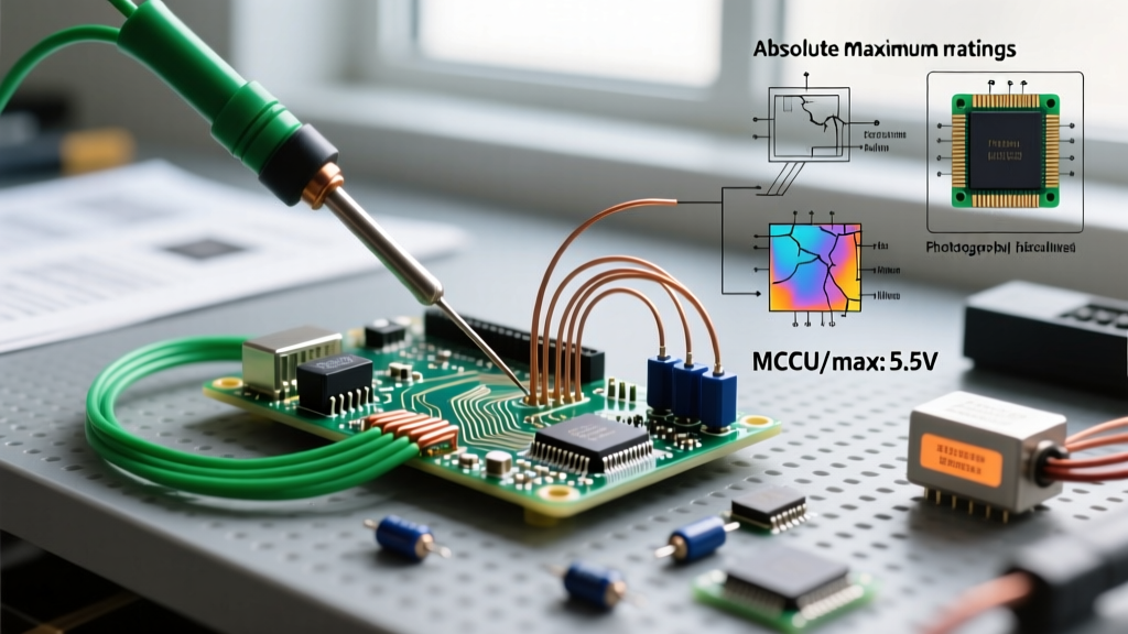
Every datasheet contains a table labeled 'Absolute Maximum Ratings,' usually accompanied by a standard boilerplate warning. Here is a typical example:
'Stresses above those listed under Absolute Maximum Ratings may cause permanent damage to the device. Exposure to absolute maximum rating conditions for extended periods may affect reliability.'
Many designers mistakenly believe that operating a component just below its absolute maximum rating is safe. In reality, this is a fast track to latent failures. Let us look at the ubiquitous STMicroelectronics STM32F103C8T6 microcontroller.
- Recommended Operating Voltage (VDD): 2.0V to 3.6V
- Absolute Maximum VDD: 4.0V
If your power supply experiences a transient spike to 3.8V, the microcontroller will likely continue to execute code. However, you have exceeded the recommended operating conditions and are now accelerating Time-Dependent Dielectric Breakdown (TDDB). The silicon dioxide gate oxides inside the IC are incredibly thin (often just a few nanometers). Operating at 3.8V increases the electric field stress across these oxides, creating microscopic traps that eventually link up to form a conductive path, resulting in a sudden, catastrophic short circuit weeks or months later.
Actionable Forensic Step:
When analyzing a failed IC that shows signs of internal shorting (low impedance between VDD and GND pins), pull the datasheet and check the Recommended Operating Conditions, not just the Absolute Maximums. If your oscilloscope captures show voltage ringing that breaches the recommended limits—even if it stays below the absolute maximum—you have found your root cause.
Thermal Resistance: Decoding θ_JA and θ_JC
Thermal runaway is one of the most common culprits in power electronics failure. To diagnose this, you must understand the thermal resistance metrics provided in the datasheet, specifically Junction-to-Ambient (θ_JA) and Junction-to-Case (θ_JC). As detailed in Texas Instruments' comprehensive guide on IC Package Thermal Metrics, these values are highly dependent on PCB layout and copper area.
Consider the classic TI LM317 linear regulator in a TO-220 package. The datasheet typically lists a θ_JA of roughly 50°C/W (when mounted on a standard JEDEC test board with minimal copper) and a θ_JC of about 4°C/W.
The Failure Math:
Suppose you are using the LM317 to drop a 12V input down to 3.3V to power a sensor array drawing 400mA.
- Voltage Drop: 12V - 3.3V = 8.7V
- Power Dissipation (Pd): 8.7V × 0.4A = 3.48W
- Temperature Rise (ΔT): 3.48W × 50°C/W (θ_JA) = 174°C
If your ambient temperature is 25°C, the silicon junction will reach 199°C. This vastly exceeds the typical 125°C to 150°C maximum junction temperature (T_J). The LM317 will trigger its internal thermal shutdown, cool down, turn back on, and repeat this cycle rapidly. This 'thermal hiccupping' causes massive output voltage ripple, which can destroy downstream sensitive RF or analog components.
Datasheet Derating Protocol:
For reliable operation, consult the NASA Electronic Parts and Packaging (NEPP) Program derating guidelines. NASA recommends derating power dissipation to 50% of the calculated maximum limit for commercial-grade silicon in harsh environments. If your datasheet math shows a junction temperature exceeding 100°C, the failure is a design flaw, not a defective batch of components.
The MLCC DC Bias Trap and Mechanical Fractures
Multilayer Ceramic Capacitors (MLCCs) are notorious for causing system-level failures when their datasheet nuances are ignored. Two specific datasheet sections are critical for failure analysis: DC Bias Characteristics and Flex Cracking limits.
1. The DC Bias Capacitance Drop
If you specify a 10µF, 16V X5R MLCC (such as the Murata GRM21BR61A106KE44) for the output filter of a 12V buck converter, you might assume you have 10µF of capacitance. However, as outlined in Murata's MLCC technology documentation, Class II dielectrics (X5R, X7R) exhibit severe capacitance loss under DC bias. At 12V, that '10µF' capacitor might only provide 2.5µF of effective capacitance.
The Failure Mode: The reduced capacitance shifts the LC double-pole frequency of your buck converter's output filter. This destroys the phase margin of the control loop, causing the regulator to oscillate wildly. The resulting overvoltage spikes can instantly blow out the gate oxides of downstream MOSFETs or fry microcontrollers.
2. Flex Cracking and Board Bending
MLCCs are brittle. When a PCB is singulated (broken apart from the panel) or when a large connector is pressed into the board, the PCB flexes. If an MLCC is placed too close to the board edge or a mounting hole, the mechanical stress transfers into the ceramic body, causing microscopic internal cracks. Over time, moisture ingress and voltage cause these cracks to arc internally, resulting in a dead short and potentially a localized fire.
Forensic Tip: If an MLCC fails short and exhibits a dark, burnt crater, cross-section the component. If the crack originates from the bottom edge near the solder fillet and angles upward at 45 degrees, it is a mechanical flex crack. You must then review your PCB layout against the manufacturer's recommended 'keep-out' zones.
Forensic Matrix: Mapping Symptoms to Datasheet Specs
Use this structured matrix to quickly correlate physical board-level symptoms with the specific datasheet parameters you need to audit during your electronic component failure analysis.
| Physical Symptom | Suspected Component | Datasheet Parameter to Audit | Verification Method |
|---|---|---|---|
| IC randomly resets under load | LDO or Buck Converter | Transient Response & Dropout Voltage | Scope VCC rail during load step; check for droop exceeding brownout threshold. |
| MOSFET overheating at idle | N-Channel MOSFET | R_DS(on) at specific V_GS (Gate Drive) | Verify gate drive voltage. A 5V logic drive on a 10V-rated MOSFET drastically increases R_DS(on). |
| Oscillator fails to start | Quartz Crystal | Drive Level (µW) & Load Capacitance (pF) | Calculate negative resistance margin; ensure inverter drive level does not overdrive the crystal. |
| Capacitor vents or explodes | Electrolytic Capacitor | Ripple Current Rating & ESR vs. Temp | Measure AC ripple current with a current probe; compare against datasheet max at operating frequency. |
| IC fails after wave soldering | Moisture Sensitive ICs | MSL (Moisture Sensitivity Level) | Check IPC/JEDEC J-STD-020 rating; verify floor life expiration before reflow. |
Moisture Sensitivity Levels (MSL) and the 'Popcorn' Effect
Not all failures happen in the field; many occur on the assembly line. If an IC package delaminates or cracks during reflow soldering, you are likely dealing with a Moisture Sensitivity Level (MSL) violation.
Plastic IC packages are slightly porous and absorb ambient humidity. When the package is subjected to the 240°C+ temperatures of lead-free reflow soldering, the trapped water instantly turns to steam. The rapid expansion of steam creates immense internal pressure, causing the package to bulge, crack, or delaminate from the silicon die—a phenomenon known as the 'popcorn effect.' This severs the delicate gold bond wires connecting the silicon to the external pins.
Datasheet Breakdown for MSL:
Check the 'Ordering Information' or 'Packaging' section at the very end of the datasheet. Components are rated from MSL 1 (unlimited floor life) to MSL 6 (mandatory bake before reflow). If your failure analysis reveals an IC with an open-circuit pin but no external burn marks, X-ray the package. If you see a cracked die paddle or severed bond wires, cross-reference the component's MSL rating with your factory's floor-life tracking logs.
Conclusion: Read the Fine Print
Effective electronic component failure analysis requires a paradigm shift. You must stop viewing the datasheet as a simple menu of features and start treating it as a strict legal contract defining the physical limits of the silicon, ceramic, and metal inside the package. By rigorously auditing absolute maximums, thermal impedances, DC bias curves, and environmental ratings, you can transition from reactive troubleshooting to proactive, bulletproof circuit design.