
When designing embedded systems, power distribution networks, or automotive electronics, choosing the right switching topology is critical. While NPN transistors and N-channel MOSFETs dominate low-side switching applications, the PNP transistor remains the undisputed king of high-side switching. In this comprehensive circuit application tutorial, we will move beyond basic theory and explore real-world PNP implementations, component selection matrices, and a critical microcontroller interfacing trap that destroys thousands of prototypes every year.
The Core Mechanics of PNP Bipolar Junction Transistors
Unlike its NPN counterpart, which relies on electron flow, a PNP bipolar junction transistor (BJT) operates primarily through the movement of positive charge carriers, known as 'holes'. For a PNP transistor to enter the active or saturation region, the base-emitter junction must be forward-biased. This means the voltage at the base must be at least 0.7V lower than the voltage at the emitter (Veb ≈ 0.7V).
Conventional current flows into the emitter and out of the collector and base. This fundamental polarity difference dictates why PNP transistors are naturally suited for sourcing current to a load, rather than sinking it to ground. According to the SparkFun Transistor Tutorial, understanding this current direction is the first step in avoiding catastrophic reverse-biasing in your PCB layouts.
Why High-Side Switching Demands a PNP Transistor
In high-side switching, the transistor is placed between the positive voltage supply (Vcc) and the load. The load is then connected directly to ground. Why is this architecture necessary? Consider an automotive fuel pump or an industrial 4-20mA sensor. If you switch the ground side (low-side) using an NPN transistor, the load remains permanently connected to the high voltage. This creates a severe short-circuit hazard if the load's chassis accidentally grounds out.
By utilizing a PNP transistor for high-side switching, the load remains completely unpowered and safely at 0V until the transistor is explicitly triggered. Furthermore, high-side switching prevents 'floating grounds,' ensuring that the load's ground reference remains stable and identical to the microcontroller's ground plane, which is vital for accurate ADC readings.
Component Selection Matrix: 2N3906 vs. BC327 vs. TIP32C
Selecting the correct PNP transistor depends heavily on your load's current draw and the available board space. Below is a comparison of three industry-standard PNP BJTs frequently used in prototyping and production PCBs.
| Part Number | Package | Max Ic (Collector Current) | Max Vceo | Typical hFE (Gain) | Est. Price (per 1k) |
|---|---|---|---|---|---|
| 2N3906 | TO-92 | 200 mA | 40 V | 100 - 300 | $0.04 |
| BC327 | TO-92 | 800 mA | 45 V | 100 - 630 | $0.06 |
| TIP32C | TO-220 | 3.0 A | 100 V | 10 - 50 | $0.45 |
Note: Always consult the specific manufacturer's datasheet, such as the ON Semiconductor 2N3906 Datasheet, to verify Safe Operating Area (SOA) limits and thermal derating curves before finalizing your BOM.
The 3.3V Microcontroller Trap (Critical Failure Mode)
Here is where most junior engineers and hobbyists fail. Imagine you are using a 3.3V microcontroller (like an ESP32 or STM32) to control a 12V relay using a 2N3906 PNP transistor in a high-side configuration.
The emitter is tied to 12V. To turn the transistor OFF, you set the MCU GPIO pin HIGH (3.3V). The voltage across the base-emitter junction (Veb) is now 12V - 3.3V = 8.7V. This will destroy your transistor.
Expert Insight: Most small-signal PNP transistors have a maximum reverse base-emitter breakdown voltage (Vebo) of only 5V. Applying 8.7V in reverse bias will cause avalanche breakdown, permanently degrading the hFE gain and eventually causing the transistor to fail short-circuit.
The Solution: NPN Level-Shifting Driver
To safely interface a 3.3V logic signal with a 12V PNP high-side switch, you must use an NPN transistor (like a 2N3904) as a level-shifting driver. The NPN pulls the PNP's base to ground, turning it ON, and isolates the MCU from the 12V rail when turning it OFF.
- MCU Pin LOW (0V): NPN is OFF. The PNP base is pulled up to 12V via a 10kΩ resistor. Veb = 0V. PNP is OFF.
- MCU Pin HIGH (3.3V): NPN turns ON and saturates. The NPN collector pulls the PNP base down to near 0V. Veb ≈ 12V. The PNP turns ON and powers the 12V load.
Calculating the Compound Driver Resistors
Let's calculate the resistors for driving a 12V relay with a 400Ω coil (30mA load current) using the NPN-PNP compound circuit.
1. PNP Base Resistor (Rb_PNP):
Assuming a forced beta (hFE) of 10 for hard saturation, we need 3mA of base current. The voltage drop across Rb_PNP is 12V - 0.7V (PNP Veb) - 0.2V (NPN Vce_sat) = 11.1V.
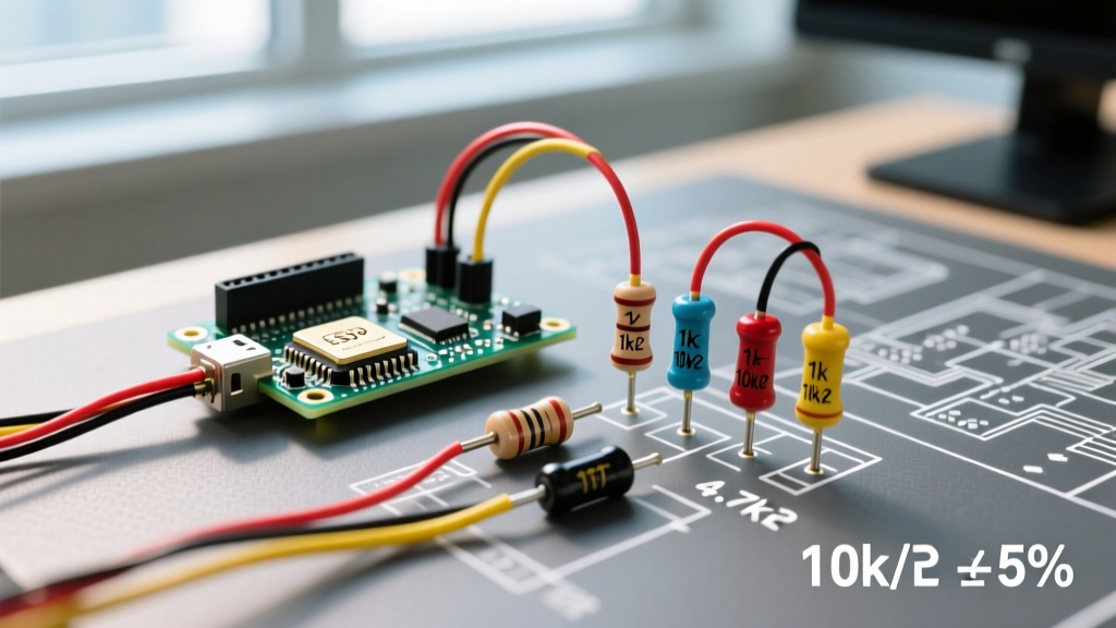
R = 11.1V / 3mA = 3.7kΩ. Use a standard 3.3kΩ or 3.9kΩ resistor.
2. NPN Base Resistor (Rb_NPN):
The NPN must sink the 3mA from the PNP base, plus a little margin. Let's aim for 4mA NPN collector current. With a forced beta of 10, we need 0.4mA NPN base current. The MCU outputs 3.3V, minus 0.7V (NPN Vbe) = 2.6V.
R = 2.6V / 0.4mA = 6.5kΩ. Use a standard 4.7kΩ resistor to guarantee deep saturation.
Prototyping and Thermal Management
When moving from the breadboard to a soldered prototype, thermal management becomes a primary concern. While a 2N3906 in a TO-92 package can dissipate roughly 625mW in free air, switching a 500mA load with a Vce(sat) of 0.4V will generate 200mW of heat. This is within limits, but if you are using a TIP32C in a TO-220 package for a 2A motor, a Vce(sat) of 1.0V generates 2 Watts of heat. Without a heatsink, the junction temperature will exceed the 150°C maximum limit in seconds, triggering thermal runaway.
For high-current PNP applications, consider replacing the BJT with a P-Channel MOSFET (like the IRF9540N) to eliminate base current requirements and drastically reduce conduction losses (I²R heating based on Rds_on).
Troubleshooting Common Breadboard Issues
If your PNP circuit is behaving erratically on a solderless breadboard, check for these specific failure modes:
- Floating Bases: Never leave the base of a PNP transistor unconnected. Parasitic capacitance and electromagnetic interference (EMI) can induce enough voltage to partially turn on the transistor, causing it to overheat. Always use a 10kΩ pull-up resistor from Base to Emitter.
- Missing Flyback Diodes: If your load is inductive (relays, solenoids, motors), the collapsing magnetic field will generate a massive reverse voltage spike when the PNP turns off. This spike will punch through the collector-base junction. Always place a 1N4148 or 1N4007 diode in reverse bias across the load.
- Parasitic Oscillation: Long breadboard wires acting as antennas can cause high-frequency oscillation in the transistor. Keep base resistor leads as short as physically possible, and place a 100pF ceramic capacitor between the base and collector if ringing is observed on your oscilloscope.
Summary and Next Steps
Mastering the PNP transistor is essential for robust, industrial-grade circuit design. By understanding the physics of hole flow, respecting the Vebo breakdown limits when interfacing with modern 3.3V logic, and properly calculating compound driver networks, you can build high-side switches that survive the harsh realities of real-world deployment. For further reading on semiconductor physics and advanced biasing networks, refer to the comprehensive guides available at Electronics Tutorials.