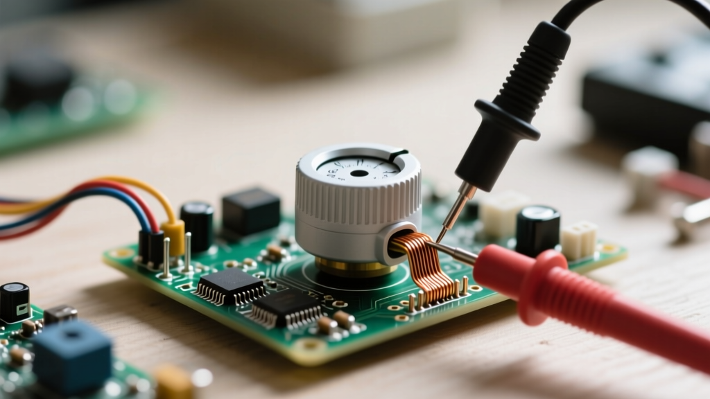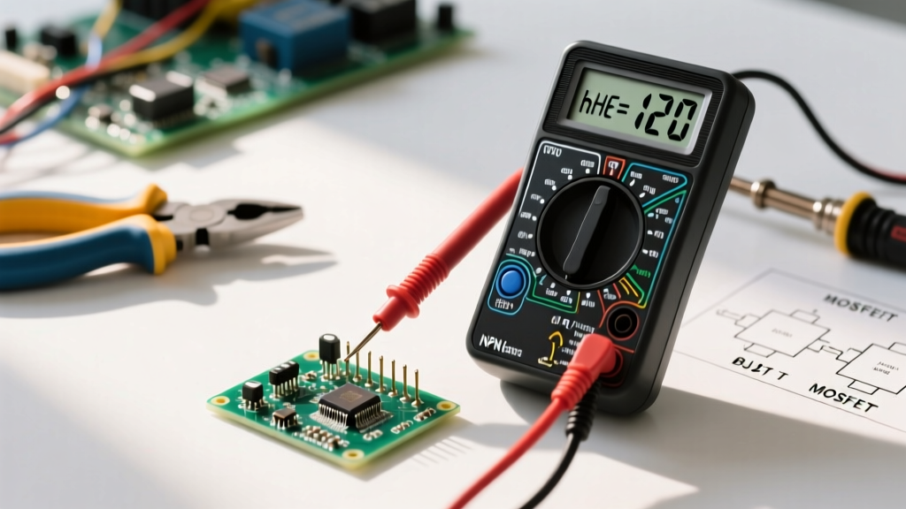

If you are troubleshooting a blown audio amplifier, a failed switching power supply, or a burnt motor driver, you might find yourself staring at a blackened semiconductor and asking: how do i test a transistor? Transistors are the fundamental building blocks of modern electronics, acting as switches and amplifiers. When they fail, they often take surrounding components with them. Knowing how to accurately test them using a standard digital multimeter (DMM) is a critical skill for any DIY electronics enthusiast or professional repair technician.
Before we dive into the probing techniques, there is one golden rule of semiconductor testing: always remove the transistor from the circuit. In-circuit testing is notoriously unreliable because parallel resistances, capacitors, and other semiconductor junctions will skew your multimeter readings, leading to false positives or missed shorts. Desolder the component, clean the pins, and test it on your bench.
The Core Physics: Why We Use Diode Test Mode
To understand how to test a transistor, you must first understand its internal architecture. A Bipolar Junction Transistor (BJT) is not a mystical three-terminal black box; it is essentially two PN-junction diodes sharing a common terminal (the Base). Because of this, the most effective way to test a BJT is by using the Diode Test mode on your digital multimeter.
On a high-quality DMM like the Fluke 87V or a reliable budget option like the Klein Tools MM400, the diode test mode applies a small, constant current (usually around 1mA to 2mA) through the probes and measures the resulting voltage drop across the junction. A healthy silicon PN junction will exhibit a forward voltage drop between 0.500V and 0.800V. If the junction is reverse-biased, the meter should display 'OL' (Over Limit) or an open circuit. By systematically testing the junctions, we can determine the transistor's health and even identify its pinout if the markings are rubbed off.
Step-by-Step: Testing Bipolar Junction Transistors (BJTs)
Whether you are holding a ubiquitous 2N3904 (NPN) or a BC557 (PNP), the testing methodology remains the same. You are looking for two functional diodes and one isolated junction.
The Six-Probe Permutation Method
A BJT has three pins: Base (B), Collector (C), and Emitter (E). Since you might not know which pin is which, or whether it is NPN or PNP, you must test all possible combinations. Place your black probe on one pin and your red probe on the second pin. Note the reading. Swap the probes. Repeat this for all three pairs of pins (1-2, 2-3, 1-3). You will perform a total of six measurements.
- Two measurements should show a forward voltage drop (typically 0.6V to 0.7V for silicon).
- Four measurements should read 'OL' (open circuit).
If you find the pin that, when touched by the red probe, yields a 0.6V drop to the other two pins (with the black probe on those other pins), you have found the Base of an NPN transistor. Conversely, if the black probe on a single pin yields a 0.6V drop to the other two pins, you have found the Base of a PNP transistor. This technique is brilliantly detailed in the semiconductor chapters of All About Circuits.
Silicon vs. Germanium Voltage Drops
While most modern transistors are silicon-based, you may encounter vintage germanium transistors (like the AC128) in old guitar pedals or radios. Germanium junctions have a much lower forward voltage drop, typically between 0.200V and 0.300V. If your DMM reads ~0.25V on two junctions, do not assume the transistor is shorted; you are likely holding a germanium device.
Distinguishing Collector from Emitter
The diode test mode will identify the Base and the transistor type (NPN/PNP), but it will not easily distinguish the Collector from the Emitter, as both junctions will read roughly the same voltage drop. To differentiate them, you can use the multimeter's hFE socket (discussed below) or rely on the datasheet for the specific part number. In some power transistors, the Collector is physically tied to the metal tab or case, which provides a mechanical clue.
Testing Power MOSFETs: Gate Capacitance and Body Diodes
Testing a MOSFET (Metal-Oxide-Semiconductor Field-Effect Transistor) like the popular IRFZ44N or IRF3205 requires a completely different approach. MOSFETs are voltage-controlled devices with an insulated Gate. Between the Gate and the Source/Drain, there is no PN junction; there is a capacitor. Therefore, a diode test between the Gate and any other pin should always read 'OL' in both directions. If it reads a voltage drop or a short, the gate oxide layer is punctured, and the MOSFET is destroyed.
The Body Diode Test
Between the Drain and the Source, power MOSFETs possess an intrinsic 'body diode' formed during the manufacturing process. For an N-channel MOSFET, the cathode of this diode is at the Drain, and the anode is at the Source. Place your red probe on the Source and black probe on the Drain; you should read a standard diode drop (~0.5V). Reverse the probes, and it should read 'OL'.
The 9V Battery Gate-Charge Trick
Because the Gate acts as a capacitor, you can actively turn the MOSFET on and off with your multimeter to verify it is functioning. According to Fluke's official testing guidelines, you can use the DMM's diode test voltage to charge the gate, but a 9V battery is often more reliable for logic-level and standard power MOSFETs.
- Discharge the gate by touching all three pins together with your finger or a piece of wire.
- Verify the body diode reads correctly (Source to Drain shows ~0.5V, Drain to Source shows 'OL').
- Touch the positive terminal of a 9V battery to the Gate and the negative terminal to the Source. This charges the gate capacitance.
- Remove the battery. Now, measure from Drain to Source with your multimeter in continuity or resistance mode. It should read near 0 ohms (the MOSFET is turned ON).
- Touch the Gate to the Source again to discharge it. The Drain-Source path should immediately return to 'OL' (the MOSFET is turned OFF).
Pro Tip: MOSFETs are highly sensitive to Electrostatic Discharge (ESD). Always touch a grounded metal surface before handling bare MOSFETs to prevent zapping the delicate gate oxide layer with static electricity from your body.
The Truth About Multimeter hFE Sockets
Many digital multimeters feature a transistor testing socket labeled 'hFE' (DC Current Gain). You plug the transistor into the NPN or PNP side, and the meter displays a number (e.g., 250). While this seems convenient, it is fraught with limitations.
First, the hFE socket applies a very low test current, usually around 10 microamps. A power transistor designed to handle 10 Amps (like a 2N3055) will exhibit a drastically lower, inaccurate hFE at such low test currents. Second, the socket cannot test transistors with built-in protection diodes or resistors. For example, if you test a TIP120 (a Darlington pair transistor) in an hFE socket, the reading will often be erratic or completely wrong because the internal base-emitter shunt resistor interferes with the meter's measurement circuit. For precise gain matching in audio amplifiers, you are much better off building a simple breadboard test jig with a known base resistor and measuring the voltage drop across a collector resistor to calculate Beta manually, as suggested by Electronics Tutorials.
Common Transistor Failure Modes in the Wild
Transistors rarely fail 'halfway'. They usually fail catastrophically due to thermal runaway, overvoltage spikes, or exceeding their Safe Operating Area (SOA). Here is how those physical failures translate to multimeter readings:
| Failure Mode | Physical Cause | Multimeter Diode Test Reading |
|---|---|---|
| Collector-Emitter Short | Thermal runaway, exceeding max Vce | 0.000V (or continuity beep) between C and E in both directions. |
| Base-Emitter Junction Open | Excessive base current, bond wire melt | 'OL' in both directions between B and E. |
| Leaky Junction | Heat degradation, silicon crystal damage | Reads a voltage drop (e.g., 0.3V) in the reverse-bias direction instead of 'OL'. |
| Gate Oxide Puncture (MOSFET) | ESD strike, Vgs overvoltage spike | Low resistance or diode drop between Gate and Source/Drain. |
Summary Table: Expected Multimeter Readings
Keep this quick-reference table on your workbench when sorting through your component bins or diagnosing a faulty PCB.
| Transistor Type | Probe Configuration | Expected Healthy Reading |
|---|---|---|
| NPN BJT | Red on Base, Black on C or E | 0.500V - 0.800V |
| NPN BJT | Black on Base, Red on C or E | 'OL' (Open) |
| PNP BJT | Black on Base, Red on C or E | 0.500V - 0.800V |
| PNP BJT | Red on Base, Black on C or E | 'OL' (Open) |
| N-Channel MOSFET | Red on Source, Black on Drain | 0.400V - 0.600V (Body Diode) |
| N-Channel MOSFET | Any probe on Gate | 'OL' (Open) |
Mastering the art of the multimeter diode test transforms a confusing pile of three-legged components into a predictable, manageable inventory. By understanding the underlying PN junctions and gate capacitances, you will never have to guess whether a transistor is the culprit in your next electronics repair.