
The Anatomy of SPI Interface Pins: Beyond the Standard 4-Wire Setup
The Serial Peripheral Interface (SPI) remains the undisputed champion for high-speed, short-distance communication between microcontrollers and peripheral ICs like flash memory, TFT displays, and ADCs. Unlike I2C, which relies on open-drain architectures and pull-up resistors, SPI interface pins operate on a push-pull topology. This allows for significantly higher clock speeds—often exceeding 50 MHz on modern 32-bit architectures—but it also demands rigorous attention to signal integrity and logic level matching.
To properly configure SPI, you must understand the four primary hardware lines:
- MOSI (Master Out Slave In): Also known as COPI (Controller Out Peripheral In) in modern nomenclature. The master generates the data signal on this pin.
- MISO (Master In Slave Out): Also known as CIPO. The peripheral sends data back to the master on this line.
- SCK (Serial Clock): The heartbeat of the bus, generated exclusively by the master to synchronize data shifting.
- CS/SS (Chip Select / Slave Select): An active-low pin used to address individual peripherals. Unlike the shared MOSI/MISO/SCK lines, CS must be routed individually to every target device.
Expert Insight: While standard SPI uses four wires, high-performance applications often require additional SPI interface pins for hardware flow control, such as a Data Ready (DRDY) interrupt pin or a Write Protect (WP) pin on flash memory modules.
Step-by-Step Wiring Guide for Standard 8-Bit AVR (Arduino UNO/Nano)
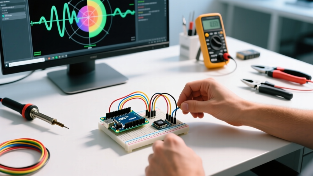
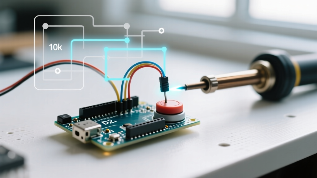
When working with 8-bit AVR microcontrollers like the ATmega328P found on the Arduino UNO, the SPI interface pins are hardcoded to specific hardware ports. While software SPI (bit-banging) is possible on any GPIO, utilizing the hardware SPI peripheral is mandatory for achieving speeds above 1 MHz without overwhelming the CPU.
ATmega328P SPI Pinout Mapping
| SPI Function | Arduino UNO Digital Pin | ICSP Header Pin | AVR Port Register |
|---|---|---|---|
| MOSI | 11 | 4 | PB3 |
| MISO | 12 | 1 | PB4 |
| SCK | 13 | 3 | PB5 |
| SS (Hardware) | 10 | - | PB2 |
Critical Wiring Rule: Even if you use a different digital pin for your Chip Select (CS) line, the hardware SS pin (Pin 10 on the UNO) must be configured as an OUTPUT in your setup code. If Pin 10 is left as an INPUT and is pulled low by external noise, the ATmega328P will automatically drop into SPI Slave mode, completely freezing your master sketch. For deeper implementation details, refer to the official Arduino SPI Reference.
Adapting SPI Interface Pins for 32-Bit Architectures (ESP32 & STM32)
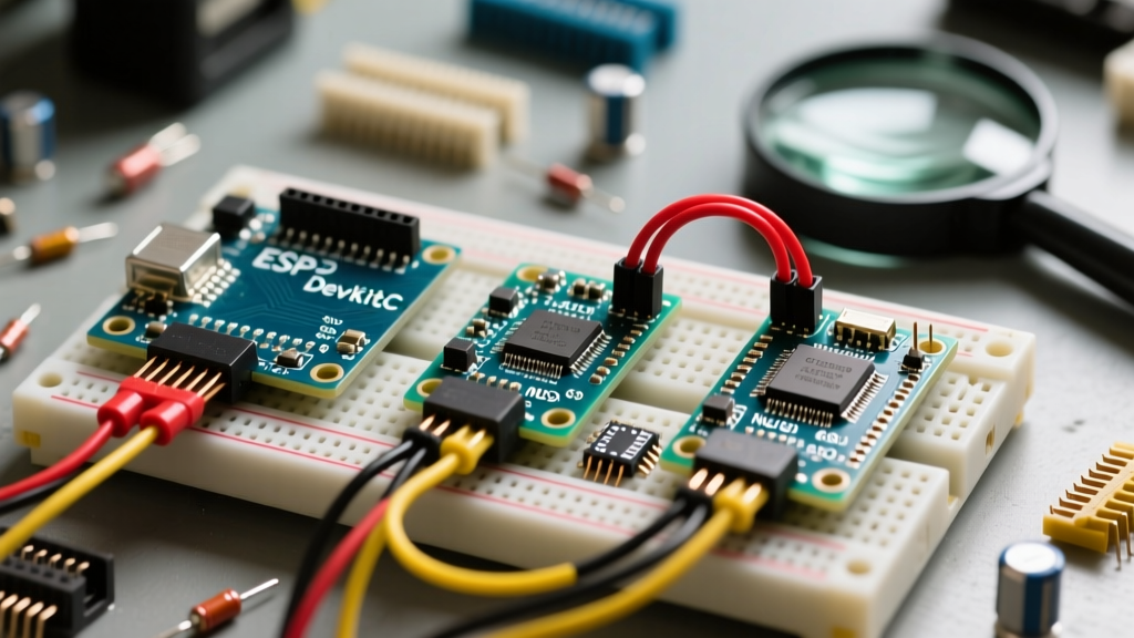
Moving to 32-bit microcontrollers introduces pin multiplexing, allowing you to route SPI interface pins to multiple GPIO pads. The ESP32, for instance, features two general-purpose SPI buses available to the user: VSPI and HSPI.
ESP32 Default SPI Bus Mappings
| Function | VSPI (Default SPI Bus) | HSPI (Secondary SPI Bus) |
|---|---|---|
| MOSI | GPIO 23 | GPIO 13 |
| MISO | GPIO 19 | GPIO 12 |
| SCK | GPIO 18 | GPIO 14 |
| CS | GPIO 5 | GPIO 15 |
When utilizing the ESP32, you can leverage the Espressif SPI Master Driver to map these SPI interface pins to alternative GPIOs via the internal GPIO matrix. However, routing high-frequency SPI signals (>20 MHz) through the GPIO matrix can introduce slight timing jitter. For ultra-high-speed peripherals like 8-bit parallel TFTs driven via SPI, always prefer the dedicated native IO_MUX pins listed above.
Troubleshooting Signal Integrity and Logic Level Mismatches
The most common point of failure when wiring SPI interface pins is ignoring logic voltage thresholds. Connecting a 5V Arduino directly to a 3.3V sensor (like a BME280 or an SD card breakout) will degrade the peripheral's lifespan or destroy it instantly via gate oxide breakdown.
The Level-Shifting Trap: Why I2C Shifters Fail on SPI
Many makers attempt to use cheap BSS138-based bidirectional level shifters designed for I2C to translate 5V SPI signals down to 3.3V. This is a critical mistake for high-speed SPI.
I2C is an open-drain protocol; the level shifter relies on pull-up resistors to bring the voltage high. SPI, however, is a push-pull protocol. The active pull-up on a BSS138 I2C shifter is too weak (often 10kΩ) to charge the parasitic capacitance of the SPI interface pins and breadboard traces quickly enough. At 4 MHz or higher, the 3.3V rising edges will look like slow, sloping ramps, causing the peripheral to misread clock pulses and corrupt data.
The Solution: Use a dedicated push-pull logic translator with active drive capabilities, such as the Texas Instruments SN74LVC1T45 (single bit) or SN74LVCH8T245 (8-bit). These ICs can source and sink the necessary current to maintain sharp square waves on SPI interface pins well past 50 MHz. For a comprehensive overview of SPI electrical characteristics, review the Analog Devices Introduction to SPI.
Bus Capacitance and Trace Length
SPI was designed for on-board communication, not long-distance cabling. The total bus capacitance (the sum of the MCU pin capacitance, trace capacitance, and peripheral input capacitance) should ideally remain under 50 pF. If you must route SPI interface pins over ribbon cables longer than 10 cm, you will encounter severe ringing and ground bounce. In these scenarios, you must terminate the lines with series resistors (typically 22Ω to 33Ω) placed as close to the master's output pins as possible to dampen reflections.
Optimizing SPI Clock Speeds and Mode Configurations
Simply wiring the SPI interface pins correctly is only half the battle; you must configure the clock polarity (CPOL) and clock phase (CPHA) to match the peripheral's datasheet. These two parameters define the four standard SPI modes.
SPI Mode Truth Table
| SPI Mode | CPOL (Clock Polarity) | CPHA (Clock Phase) | Idle State | Data Sampled On |
|---|---|---|---|---|
| Mode 0 | 0 | 0 | Low | Rising Edge |
| Mode 1 | 0 | 1 | Low | Falling Edge |
| Mode 2 | 1 | 0 | High | Falling Edge |
| Mode 3 | 1 | 1 | High | Rising Edge |
Pro-Tip: If your SPI peripheral is returning shifted or garbage data, but the wiring is verified, you are likely using the wrong SPI Mode. Mode 0 and Mode 3 are the most common in modern flash and sensor ICs. Always initialize your bus at a low speed (e.g., 1 MHz) during development, verify the data payload via a logic analyzer, and then incrementally increase the clock divider (e.g., SPI_CLOCK_DIV2) to find the maximum stable bandwidth.
Final Checklist Before Powering Your SPI Bus
Before uploading your sketch and applying power, run through this hardware verification checklist to protect your microcontroller and peripherals:
- Verify Logic Levels: Are 3.3V and 5V domains separated by a proper push-pull level shifter?
- Check CS Routing: Does every peripheral have its own dedicated Chip Select pin? (Never wire multiple CS pins together unless utilizing a hardware multiplexer).
- Confirm Common Ground: All SPI interface pins require a shared, low-impedance ground reference. Ensure the GND wire is at least as thick as the VCC wire.
- Hardware SS Pin State: If using an 8-bit AVR, is the hardware SS pin set to
OUTPUTin software, or physically pulled high via a 10kΩ resistor? - Decoupling Capacitors: Is there a 100nF ceramic capacitor placed physically adjacent to the VCC and GND pins of the SPI peripheral IC?
By respecting the electrical realities of push-pull buses and carefully mapping your SPI interface pins to the correct hardware peripherals, you will eliminate the vast majority of communication errors and unlock the full, high-speed potential of your microcontroller projects.