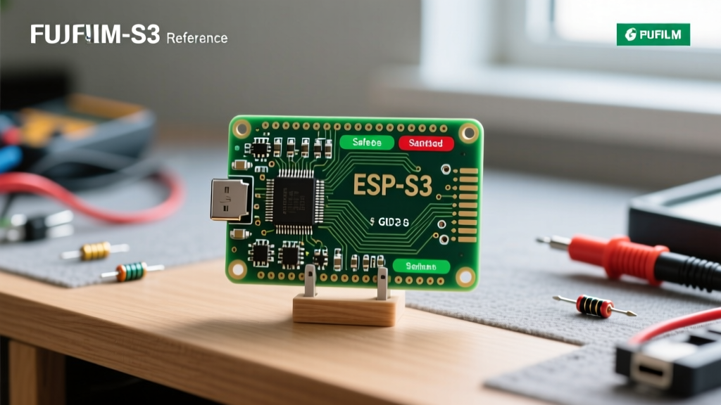

The ESP32-S3 Architecture: Beyond the Original
The ESP32-S3 represents a massive leap in Espressif's microcontroller lineup, introducing dual-core Xtensa LX7 processors running at 240 MHz, native USB OTG support, and vector instructions for AI acceleration. However, these upgrades fundamentally alter the esp32s3 pinout compared to the original ESP32. Makers and hardware engineers frequently encounter boot failures, erratic ADC readings, or bricked modules because they apply legacy ESP32 wiring logic to the S3 variant.
This quick-reference FAQ and hardware guide is designed to help you navigate the ESP32-S3 GPIO matrix, avoid critical strapping pin conflicts, and design robust custom PCBs or wire up development boards like the ESP32-S3-DevKitC-1 without catastrophic failure.
Quick Reference: Which GPIOs Are Actually Safe?
Unlike the original ESP32, which hid internal flash on GPIOs 6-11, the ESP32-S3 pushes internal memory interfaces much higher up the pinout. If you are designing a breakout board or wiring sensors, use this matrix to ensure you are not conflicting with internal PSRAM or SPI Flash.
| GPIO Range | Status | Recommended Use Case |
|---|---|---|
| GPIO 0 - 21 | Safe / RTC Capable | General I/O, Touch Sensors, Deep Sleep Wake-up, ADC1 |
| GPIO 22 - 25 | Safe | General I/O, I2C, SPI peripherals |
| GPIO 26 - 32 | Restricted | Internal SPI Flash (Do not use on WROOM modules) |
| GPIO 33 - 37 | Restricted | Internal Octal SPI / PSRAM (Do not route to headers) |
| GPIO 38 - 42 | Safe | General I/O, High-speed SPI, Camera interfaces |
| GPIO 43 - 44 | Safe (Default UART) | Hardware UART0 (TX/RX via USB-UART bridge) |
| GPIO 45 - 48 | Strapping / Safe | General I/O (with boot-state caveats), RGB LEDs |
Frequently Asked Questions (FAQ)
1. What are the Strapping Pins and how do they affect boot?
The ESP32-S3 samples specific pins during the reset sequence to determine boot modes, flash voltages, and JTAG routing. If these pins are pulled to the wrong state by external sensors or motor drivers, your board will fail to boot or enter an unintended ROM bootloader state.
| Pin | Function | LOW State Behavior | HIGH State Behavior |
|---|---|---|---|
| GPIO 0 | Boot Mode | SPI Flash Boot (Normal) | ROM Bootloader (Download Mode) |
| GPIO 3 | JTAG Source | JTAG via GPIO pins | JTAG via Native USB |
| GPIO 45 | Flash Voltage | 3.3V Flash Operation | 2.4V / 1.8V Flash Operation |
| GPIO 46 | Boot Log | Silences ROM boot messages | Prints boot log to UART |
Pro-Tip for PCB Designers: Never place pull-down resistors on GPIO 45 unless you are explicitly using a 1.8V SPI flash chip. For 99% of standard 3.3V ESP32-S3-WROOM-1 modules, GPIO 45 must be left floating or pulled HIGH to prevent brownout-induced boot loops. Consult the Espressif Hardware Design Guidelines for exact resistor values.
2. How do I wire the Native USB (OTG) vs. Standard UART?
The ESP32-S3 features two distinct USB pathways on most development boards, which causes immense confusion for beginners:
- Native USB (GPIO 19 & 20): GPIO 19 is D- and GPIO 20 is D+. This connects directly to the ESP32-S3 silicon. It supports USB OTG, HID (keyboards/mice), Mass Storage, and native CDC/JTAG debugging without an external bridge chip.
- UART Bridge USB (GPIO 43 & 44): This routes to an onboard CH340 or CP2102 chip. It is strictly for standard serial monitoring and legacy auto-reset firmware flashing.
Troubleshooting Insight: If you are using the Arduino IDE and your serial monitor outputs garbage or fails to connect after a reset, ensure you have selected the correct COM port. The Native USB port and the UART Bridge port will show up as two separate COM devices in your OS device manager.
3. Why is my ADC reading erratic when Wi-Fi is active?
Just like the original ESP32, the ESP32-S3 suffers from ADC2 and Wi-Fi coexistence conflicts. The ESP32-S3 features ADC1 (GPIO 1-10) and ADC2 (GPIO 11-20). When the Wi-Fi radio initiates a transmission or scans for networks, it commandeers the ADC2 hardware multiplexer. If your analog sensor is wired to GPIO 12, your readings will drop to zero or spike randomly during network activity. Always route critical analog sensors to ADC1 (GPIO 1-10).
Default Peripheral Pin Assignments
While the ESP32-S3 allows you to map almost any peripheral to any safe GPIO via the GPIO matrix, sticking to the Arduino core defaults prevents conflicts with third-party libraries (like the TFT_eSPI or Wire libraries).
| Peripheral | Default S3 Pins | Notes |
|---|---|---|
| I2C (Wire) | SDA: GPIO 8 | SCL: GPIO 9 | Requires 4.7k pull-ups for external devices |
| SPI (VSPI) | MOSI: 11, MISO: 13, SCK: 12, CS: 10 | Verify library definitions, some map to GPIO 38-42 |
| UART0 | TX: GPIO 43 | RX: GPIO 44 | Connects to external USB-UART bridge |
| UART1 | TX: GPIO 17 | RX: GPIO 18 | Safe for GPS or secondary serial devices |
Critical Hardware Design Traps to Avoid
The Octal SPI PSRAM Conflict (GPIO 33-37)
Many makers purchase the ESP32-S3-WROOM-1U or N8R8 modules, which include 8MB of PSRAM. To achieve the bandwidth required for AI and camera buffers, Espressif uses an Octal SPI interface for the PSRAM. This interface permanently consumes GPIO 33 through 37. On the original ESP32, pins in the 30s were heavily used for capacitive touch and general I/O. On the S3, routing traces to these pins on a custom PCB will cause short circuits with the internal memory bus, resulting in immediate kernel panics and Guru Meditation errors upon boot.
Power Delivery and Brownout Resets
The ESP32-S3 is a power-hungry chip when transmitting on Wi-Fi or driving the RGB LED peripherals. Transmission spikes can exceed 350mA in microseconds. If your 3.3V voltage regulator (like a standard AMS1117-3.3) lacks sufficient transient response, or if your decoupling capacitors are placed too far from the module's 3V3 pin, the chip will experience a brownout and reset continuously.
- Bulk Capacitance: Place a 100µF to 470µF low-ESR tantalum or ceramic capacitor directly at the power entry of your ESP32-S3 module.
- Decoupling: A 100nF (0.1µF) ceramic capacitor must be placed as close to the 3V3 and GND pins of the WROOM module as physically possible to filter high-frequency RF noise.
Antenna Keep-Out Zones
If you are integrating the ESP32-S3-WROOM-1 module onto a custom PCB, the meandering PCB antenna requires a strict keep-out zone. Do not pour copper ground planes on the top or bottom layers directly beneath the antenna overhang. Furthermore, ensure no metal enclosure or battery sits within 15mm of the antenna tip, or your Wi-Fi range will degrade from 50 meters to less than 3 meters. For metallic enclosures, switch to the WROOM-1U variant and route the RF trace to an external U.FL / IPEX connector.
Authoritative Resources for Deep Dives
To ensure your designs pass FCC/CE certification and operate reliably in industrial environments, always cross-reference your pinout decisions with official silicon documentation:
- ESP32-S3 Official Datasheet - The definitive source for electrical characteristics, max current draw per GPIO (typically 40mA absolute max, 20mA recommended), and internal block diagrams.
- Espressif Hardware Design Guidelines - Mandatory reading for PCB layout, RF matching networks, and strapping pin resistor networks.
- Arduino ESP32 Core Documentation - Essential for understanding how the Arduino abstraction layer maps default peripherals and handles native USB CDC/HID configurations.
By respecting the unique architecture of the ESP32-S3 and avoiding legacy ESP32 assumptions, you can fully leverage its AI capabilities and native USB features for next-generation IoT and robotics projects.