
The Architecture Behind the ESP32 C3 Pinout
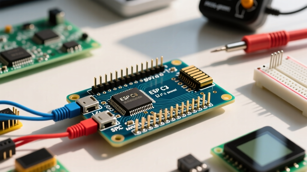
When transitioning from the classic ESP32-WROOM or the ESP8266 to the RISC-V-based ESP32-C3, hardware makers and firmware engineers often hit a hidden wall: pinout incompatibility. Understanding the ESP32 C3 pinout is not just about knowing which wire goes where; it is about optimizing your entire hardware design workflow to avoid debugging nightmares, boot failures, and peripheral conflicts. The ESP32-C3 features a single-core 32-bit RISC-V microcontroller running at up to 160 MHz, offering a compelling mix of Wi-Fi and Bluetooth 5 (LE) at a fraction of the cost and power consumption of its dual-core predecessors.
However, the physical GPIO count is strictly limited. While the silicon die supports up to 22 general-purpose I/O pins, the actual number of exposed pins depends heavily on your chosen module. For instance, the popular ESP32-C3-DevKitM-1 exposes 18 usable pins, while the ultra-compact 'SuperMini' boards often expose only 11 edge-pins to maintain a breadboard-friendly footprint. Optimizing your workflow starts with mapping these physical constraints before you ever open your schematic capture software or wire up a prototype.
Critical Strapping Pins: The Hidden Workflow Killers
The most common point of failure in rapid prototyping with this chip is ignoring the boot strapping pins. During reset, the ESP32-C3 samples specific GPIOs to determine its boot mode and logging behavior. If your external circuitry (like pull-up resistors for I2C or switches) interferes with these states, the chip will fail to boot or enter download mode unexpectedly.
| GPIO Pin | Function | Logic LOW (0) | Logic HIGH (1) |
|---|---|---|---|
| GPIO8 | Boot Mode Selection | Download Mode (UART) | SPI Flash Boot (Normal) |
| GPIO9 | Boot Log Printing | Enable Serial Log | Disable Serial Log |
| GPIO2 | SPI Flash Config | Internal Pull-down | Internal Pull-up |
Workflow Optimization Rule: Never assign GPIO8 and GPIO9 to I2C buses or external interrupt buttons without hardware isolation. A standard 4.7kΩ I2C pull-up resistor on GPIO9 will force the chip to disable boot logs, making firmware debugging incredibly frustrating. Remap your primary I2C sensors to safer GPIOs like GPIO4 (SDA) and GPIO5 (SCL).
The ADC Migration Trap: Analog Sensor Workflows
Makers migrating from the original ESP32 often assume they have access to two Analog-to-Digital Converters (ADC1 and ADC2). This assumption will break your analog sensor workflow. The ESP32-C3 only features ADC1, which is limited to 5 channels mapped to GPIO0 through GPIO4.
Expert Insight: If your project requires reading multiple analog sensors (e.g., NTC thermistors, soil moisture, or potentiometers) while simultaneously using Wi-Fi, you must reserve GPIO0-GPIO4 exclusively for ADC1. Furthermore, because GPIO2 is a strapping pin, using it for an analog sensor requires careful timing: read the ADC value only after the boot sequence has completed and the pin state is no longer being sampled by the bootloader.
To optimize analog workflows, use the ESP-IDF GPIO documentation to configure ADC1 attenuation correctly. For battery voltage monitoring, route your voltage divider to GPIO3, leaving GPIO0 and GPIO1 free for digital UART or I2C fallbacks.
Peripheral Allocation Matrix and Remapping
One of the greatest advantages of the ESP32 architecture is the GPIO Matrix, which allows most digital peripherals to be routed to almost any pin. However, relying on default Arduino core mappings can lead to suboptimal PCB routing and signal integrity issues. Here is an optimized allocation framework for a standard IoT sensor node:
- Hardware I2C (I2C0): Remap from default (8/9) to GPIO4 (SDA) and GPIO5 (SCL). This avoids strapping pin conflicts and keeps the analog pins free.
- Hardware SPI (SPI2_HOST): Use GPIO6 (MOSI), GPIO7 (MISO), GPIO10 (SCK), and GPIO20 (CS). This grouping keeps high-speed traces physically close together on a custom PCB, reducing parasitic capacitance.
- Primary UART (UART0): Stick to GPIO21 (TX) and GPIO20 (RX) for USB-CDC or primary serial debugging. The C3 features an internal USB-Serial-JTAG controller, meaning you often do not need an external CP2102 or CH340 chip, saving board space and BOM costs.
- PWM / LEDC: The C3 supports up to 6 LEDC channels. Assign these to GPIOs that are physically routed near your MOSFET gates or LED drivers to minimize EMI.
When using the Arduino Core for ESP32, you can easily redefine these pins in your setup function using Wire.begin(SDA_PIN, SCL_PIN); to enforce your optimized workflow.
Optimizing Breadboard and PCB Layouts
Physical layout dictates signal integrity, especially when dealing with the ESP32-C3's integrated 2.4GHz RF frontend. Whether you are prototyping on a breadboard or designing a 2-layer PCB in KiCad, power delivery and grounding must dictate your pinout choices.
Power Delivery and Grounding Strategies
The ESP32-C3 can draw peak currents exceeding 350mA during Wi-Fi transmission bursts. If your ground return path has high impedance, you will experience brownouts and random reboots. Workflow Tip: When wiring on a breadboard, use both ground rails. Connect one ground rail to the ESP32-C3 GND pin, and use the second ground rail exclusively for high-current peripherals like relays or neopixel strips. On a PCB, ensure a continuous ground pour on Layer 2 directly beneath the RF antenna trace and the main VDD3P3 decoupling capacitors.
For the 'SuperMini' variants, the onboard LDO is often rated for only 500mA. If your peripheral suite (e.g., an OLED display + BME280 + active buzzer) approaches this limit, bypass the onboard regulator by injecting a clean 3.3V directly into the 3V3 pin, treating the USB 5V line purely for charging or high-voltage logic shifting.
Advanced GPIO Features for Power-Saving Workflows
For battery-operated deployments, the ESP32 C3 pinout offers specific RTC (Real-Time Clock) GPIOs that remain powered during deep sleep. According to the official Espressif ESP32-C3 Datasheet, only a subset of pins can wake the chip from deep sleep. Optimize your low-power workflow by routing your wake-up buttons, PIR motion sensors, or reed switches exclusively to GPIO0, GPIO1, GPIO2, GPIO3, GPIO4, or GPIO5. If you route a wake-up interrupt to GPIO10, the chip will ignore it, and your device will sleep indefinitely until a hard reset occurs.
Pre-Flight Pinout Checklist
Before finalizing your schematic or wiring your prototype, run this 5-point optimization checklist to ensure your pinout strategy is bulletproof:
- Strapping Pin Audit: Are GPIO2, GPIO8, and GPIO9 free of external pull-ups/pull-downs that conflict with SPI boot and serial logging?
- ADC Verification: Are all analog sensors restricted to GPIO0-GPIO4 (ADC1)?
- Deep Sleep Wake Sources: Are all wake-up interrupts mapped to RTC-capable GPIOs (0-5)?
- RF Clearance: Is the antenna area (usually near GPIO1 and the module edge) completely clear of ground pours and signal traces?
- Current Budgeting: Does the total peripheral draw exceed the module's onboard LDO capacity, requiring external 3.3V regulation?
By treating the ESP32 C3 pinout not just as a list of connections, but as a system of architectural constraints and opportunities, you drastically reduce hardware iteration cycles. This systematic approach ensures that your transition from breadboard prototype to manufactured PCB is seamless, reliable, and optimized for both performance and power efficiency.