
When we think of electrical wiring, we often picture thick copper cables carrying high-voltage AC power. However, conductors in electronics operate in an entirely different realm. From microscopic traces on a printed circuit board (PCB) to nanometer-scale interconnects inside a silicon microchip, electronic conductors must manage extreme current densities, high-frequency signal propagation, and complex thermal environments. Understanding the material science and failure modes of these conductors is critical for any electronics designer, DIY engineer, or hardware troubleshooter.
The Quantum Mechanics of Electronic Conduction
Before selecting a material, it is essential to understand why certain elements conduct electricity while others act as insulators. According to band theory in solid-state physics, electrons in a solid occupy specific energy levels grouped into "bands." The valence band contains electrons bound to atoms, while the conduction band contains free electrons capable of moving and carrying current.
In conductors in electronics like copper and silver, the valence and conduction bands overlap. This overlap means that even at room temperature, a massive sea of delocalized electrons is available to drift under an applied electric field. In contrast, insulators have a wide "band gap" between these zones, requiring immense energy to free an electron. Semiconductors sit in the middle, with a narrow band gap that can be manipulated via doping—a foundational concept for active components like transistors.
The Big Four: Primary Conductive Materials Profiled
While the periodic table offers dozens of metallic elements, the electronics industry relies heavily on four primary conductors, each chosen for specific electrical, mechanical, and chemical properties.
1. Copper (Cu): The Industry Standard
Copper is the undisputed baseline for electronic conduction. The International Annealed Copper Standard (IACS) sets pure annealed copper at 100% conductivity. According to the Copper Development Association, its excellent balance of high electrical conductivity, thermal dissipation, and mechanical tensile strength makes it ideal for PCB traces, transformer windings, and component leads. However, bare copper oxidizes readily in air, forming a semiconductive copper oxide layer that can ruin low-voltage contact resistance.
2. Gold (Au): The Contact King
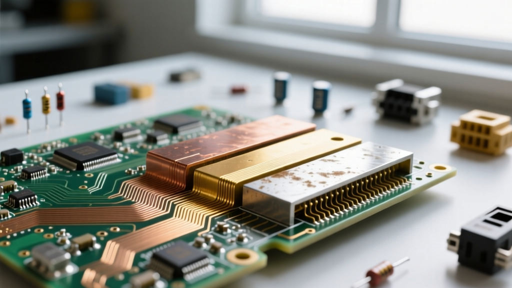
Contrary to popular belief, gold is actually a worse bulk conductor than copper (roughly 70% IACS). Its supreme value in electronics lies in its chemical inertness. Gold does not oxidize or tarnish, ensuring near-zero contact resistance over decades of use. It is the standard for edge connectors (like PCIe slots), RF switch contacts, and ultra-fine wire bonding inside integrated circuit (IC) packages.
3. Silver (Ag): The High-Frequency Specialist
Silver holds the highest electrical conductivity of all metals at roughly 105% IACS. Despite this, it is rarely used for bulk wiring because it tarnishes rapidly, forming silver sulfide—a highly resistive compound. However, in high-frequency RF and microwave circuits, silver plating is heavily utilized due to the skin effect (detailed below), where the signal travels exclusively on the extreme outer surface of the conductor.
4. Aluminum (Al): The IC Interconnect
With a conductivity of about 61% IACS, aluminum seems like a poor choice. Yet, it is historically the dominant material for on-chip metallization (the microscopic wiring inside silicon chips). Aluminum is lightweight, inexpensive, and adheres exceptionally well to silicon dioxide (SiO2) insulating layers. While modern high-end chips have largely migrated to copper interconnects to reduce RC delay, aluminum remains vital in power electronics and discrete semiconductor packaging.
Material Properties Matrix
The following table compares the fundamental properties of these conductors at 20°C, providing a quick reference for material selection in electronic design.
| Material | Resistivity (nΩ·m) | IACS (%) | Primary Electronic Application | Oxidation / Tarnish Risk |
|---|---|---|---|---|
| Silver (Ag) | 15.87 | 105% | RF/Microwave plating, specialized fuses | High (Silver Sulfide) |
| Copper (Cu) | 16.78 | 100% | PCB traces, windings, busbars | Moderate (Copper Oxide) |
| Gold (Au) | 24.40 | 70% | Edge connectors, IC wire bonding | None (Inert) |
| Aluminum (Al) | 26.50 | 61% | On-chip interconnects, electrolytic capacitors | High (Passivating Oxide) |
The High-Frequency Reality: Skin Effect and Surface Roughness
When designing conductors in electronics for high-speed digital signals or RF applications, DC resistance becomes largely irrelevant. Due to the skin effect, alternating current (AC) tends to flow primarily on the outer surface of a conductor. The skin depth ($\delta$) decreases as the frequency increases.
For example, at a DC or 60 Hz mains frequency, current utilizes the entire cross-section of a 1 oz (35 µm) copper PCB trace. However, at 10 GHz (common in 5G and Wi-Fi 6E routers), the skin depth in copper shrinks to approximately 0.66 micrometers.
Design Insight: At microwave frequencies, the microscopic roughness of the copper foil on a PCB can cause massive insertion losses. If the surface roughness (Rz) of the copper is greater than the skin depth, the signal is forced to travel a longer, jagged path, increasing effective resistance and degrading signal integrity. This is why high-frequency PCB laminates use ultra-smooth Rolled Annealed (RA) copper rather than standard Electrodeposited (ED) copper.
Micro-Scale Failure Modes: When Conductors Stop Conducting
Unlike residential wiring, which fails primarily due to thermal overload or physical severing, micro-electronic conductors fail through complex atomic-level mechanisms.
Electromigration in Micro-Traces
Electromigration is the transport of material caused by the gradual movement of the ions in a conductor due to the momentum transfer between conducting electrons and diffusing metal atoms. In modern ICs, current densities can exceed $10^6 \text{ A/cm}^2$. Over time, the "electron wind" physically pushes metal atoms down the trace. This creates voids (leading to open circuits) at the cathode end and hillocks (leading to short circuits with adjacent traces) at the anode end. Designers mitigate this by using Black's Equation to calculate mean time to failure (MTTF) and by alloying copper with small amounts of silver or manganese.
Tin Whiskers and Galvanic Corrosion
With the industry-wide shift to RoHS-compliant (lead-free) solder, pure tin finishes became standard on component leads and PCB pads. Under certain thermal and mechanical stresses, pure tin can spontaneously grow microscopic, crystalline structures known as tin whiskers. These conductive whiskers can bridge the gap between adjacent pins on a microchip, causing catastrophic short circuits in mission-critical systems like aerospace and medical devices.
Furthermore, when dissimilar metals meet in the presence of an electrolyte (even ambient humidity), galvanic corrosion occurs. If a gold-plated connector is mated with a tin-plated header, the tin will rapidly corrode, increasing contact resistance and causing intermittent signal failures. The IPC-2221 Generic Standard on Printed Board Design provides strict guidelines on avoiding dissimilar metal mating in harsh environments.
Practical Selection Framework for PCB Designers
To ensure reliability in your next electronics project, apply this decision framework when specifying conductors:
- For Power Delivery Networks (PDN): Maximize copper weight (e.g., 2 oz or 3 oz copper) and use wide, polygonal pours. Rely on the bulk thermal mass of the copper to dissipate $I^2R$ heating.
- For RF and High-Speed Digital (GHz range): Specify low-profile copper foils and consider immersion silver or ENIG (Electroless Nickel Immersion Gold) surface finishes. Remember that nickel is magnetic and can introduce losses at high frequencies; keep the nickel layer as thin as the fab house allows.
- For Harsh Environments / High-Vibration: Avoid pure tin finishes to prevent whisker growth. Opt for matte tin-lead (if exempt from RoHS) or specialized conformal coatings to block moisture-induced galvanic corrosion.
Mastering the behavior of conductors in electronics requires looking beyond simple Ohm's Law calculations. By understanding the quantum nature of the materials, the high-frequency realities of the skin effect, and the microscopic failure modes of modern manufacturing, you can design circuits that are not only functional on the bench but robust in the real world. For further reading on material properties at extreme temperatures, refer to the National Institute of Standards and Technology (NIST) superconductivity and materials databases.