
The Hidden Cost of Messy Prototyping
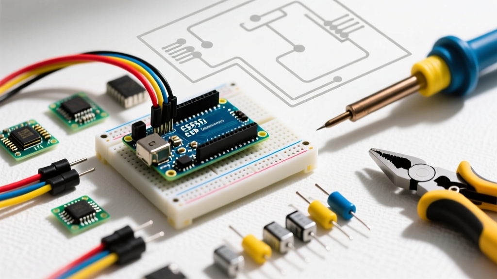
When scaling from a simple blinking LED to a complex sensor array using modern boards like the Arduino Uno R4 Minima or Nano ESP32, your physical layout dictates your debugging speed. Many makers waste hours chasing phantom I2C errors, random resets, or unexplained voltage drops, never realizing the root cause is poor physical topology. Understanding exactly how to use Arduino breadboard environments strategically is the difference between a 30-minute prototype and a 4-hour debugging nightmare. Workflow optimization on the breadboard isn't just about aesthetics; it is an engineering discipline that minimizes parasitic capacitance, prevents ground loops, and drastically reduces troubleshooting time.
In this guide, we break down the professional workflows used by hardware engineers to transform the standard solderless breadboard from a chaotic web of wires into a highly optimized, reliable prototyping platform.
Anatomy of a High-Efficiency Breadboard Layout
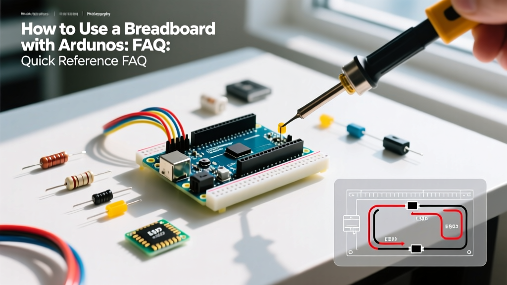
The standard 830-point breadboard (commonly sold as the MB-102 or Elegoo MB-102) features two main horizontal power rails and a central split terminal strip. The most common workflow bottleneck occurs when makers treat the power rails as an afterthought. An optimized workflow mandates a strict Power-First Routing Protocol.
The Power-First Routing Protocol
- Establish Dual Voltage Rails: Modern MCU workflows frequently mix 5V and 3.3V logic. Designate the top red/blue rails for 5V/GND and the bottom red/blue rails for 3.3V/GND. Use a physical piece of red electrical tape to mark the 5V rail and orange tape for the 3.3V rail at the edge of the board to prevent catastrophic cross-wiring.
- Bridge the Gaps Early: The power rails on an 830-point board are often split in the middle. Before placing a single IC, use a short, thick jumper to bridge the left and right halves of your ground rail. A fragmented ground plane introduces varying ground potentials, which causes analog-to-digital converter (ADC) jitter on pins like A0-A5.
- Decoupling Placement: According to the Texas Instruments SZZA009 Application Report on decoupling, capacitors must be placed as close to the IC VCC pin as physically possible. On a breadboard, this means straddling a 100nF (0.1µF) X7R ceramic capacitor directly across the power trench, no more than 3 rows away from your microcontroller's power pins.
Standardizing Your Wiring Color Code
Nothing destroys workflow momentum faster than tracing a yellow wire with a multimeter to figure out if it's carrying 5V, an I2C clock signal, or a PWM output. Standardizing your wire colors allows your brain to parse the circuit schematically at a glance. While the SparkFun Breadboard Tutorial suggests basic red/black for power, a professional 2026 workflow requires a more granular approach for complex MCU builds.
| Wire Color | Function / Signal Type | Workflow Rationale |
|---|---|---|
| Red | 5V VCC | Universal standard for primary 5V power distribution. |
| Orange | 3.3V VCC | Distinct from 5V; prevents frying 3.3V sensors like the BME280. |
| Black | Primary Ground (GND) | Universal standard for common ground returns. |
| Blue | Secondary / Analog Ground | Used for star-grounding analog sensors to reduce digital noise. |
| Yellow | I2C SDA / SPI MOSI | Data lines. High visibility for high-speed bus troubleshooting. |
| Green | I2C SCL / SPI SCK | Clock lines. Paired with yellow for instant bus identification. |
| Purple | Interrupts / Chip Select (CS) | Control lines that trigger specific hardware interrupts. |
| White/Grey | Analog Signals / PWM | Reserved for variable signals going to ADC or DAC pins. |
Pro Tip: Buy pre-formed jumper wire kits (like the 140-piece Elegoo or RexQualis sets) rather than cutting and stripping your own solid-core wire. Pre-formed wires lay flat against the breadboard surface, eliminating the 'rat's nest' effect and reducing accidental wire-snags that pull components loose during testing.
Signal Integrity: Managing I2C and SPI on Solderless Boards
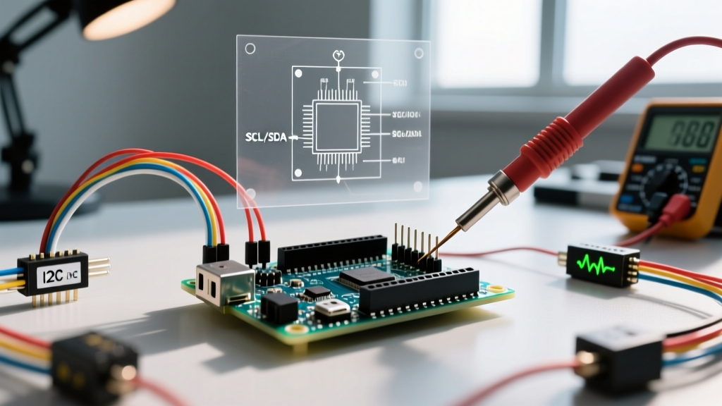
A major edge case in breadboard prototyping is signal degradation on high-speed buses. Solderless breadboards introduce significant parasitic capacitance between adjacent metal clips. When learning how to use Arduino breadboard setups for sensor networks, you must account for bus capacitance limits.
The I2C 400pF Limit
The official NXP UM10204 I2C-bus specification dictates a maximum bus capacitance of 400pF for standard and fast-mode I2C. A standard breadboard trace adds approximately 2pF to 4pF of capacitance per centimeter of wire. If you are daisy-chaining multiple I2C sensors (like an MPU6050, OLED display, and BME680) using long, looping jumper wires, you will easily exceed this limit, resulting in corrupted data packets and NACK errors.
- Optimization Rule 1: Keep I2C SDA and SCL wires under 15cm in length when operating at 400kHz.
- Optimization Rule 2: Never route I2C wires parallel to high-current PWM lines (like motor driver outputs) to prevent inductive crosstalk.
- Optimization Rule 3: If your I2C bus fails intermittently, drop the clock speed to 100kHz in your Arduino Wire library initialization (
Wire.setClock(100000);) to increase noise tolerance.
Wire Gauge and Contact Fatigue: The Physical Bottlenecks
The internal clips of a quality breadboard are made of beryllium copper or phosphor bronze, designed to grip specific wire diameters. Using the wrong wire gauge is a primary cause of intermittent connection failures.
The 22 AWG Sweet Spot
Standard breadboards are optimized for 22 AWG (0.64mm diameter) solid-core wire.
- Using 24 AWG or Stranded Wire: Stranded wire frays upon insertion, leaving tiny copper splinters that cause short circuits between adjacent rows. Furthermore, stranded wire lacks the rigidity to push past the internal clip's entry bevel, leading to false insertions where the wire feels seated but makes no electrical contact.
- Using 20 AWG or Component Leads: Forcing thick component leads (like those on heavy electrolytic capacitors or older DIP switches) into the breadboard will permanently stretch the beryllium copper clips. Once a clip is stretched beyond its yield strength, it will never securely hold a standard 22 AWG wire again.
Workflow Hack: Keep a dedicated 'sacrificial' breadboard for inserting thick component leads, or solder 22 AWG pigtail extensions to heavy components before inserting them into your primary prototyping board.
Step-by-Step Workflow: From Schematic to Physical Board
To maximize efficiency, follow this sequential build order. Do not deviate, as retrofitting power lines under signal wires is the leading cause of accidental short circuits.
- Phase 1: Power & Ground Infrastructure. Lay all red, orange, and black pre-formed wires flat against the board. Connect the main power rails to the Arduino 5V, 3.3V, and GND pins. Use a multimeter in continuity mode to verify that no power rail is shorted to ground before applying USB power.
- Phase 2: IC and Breakout Board Placement. Insert your microcontrollers and sensor modules. Ensure they straddle the central trench correctly. Leave at least two empty rows on either side of the IC for decoupling capacitors and pull-up resistors.
- Phase 3: Passive Components. Install resistors, capacitors, and LEDs. Bend resistor leads neatly and trim excess if necessary. Place pull-up resistors for I2C lines (typically 4.7kΩ) directly adjacent to the master MCU.
- Phase 4: Signal Routing. Route your yellow, green, and purple signal wires. Keep them as short and flat as possible. If two signal wires must cross, do so at a 90-degree angle to minimize capacitive coupling.
- Phase 5: The 'Tug Test' & Power Up. Gently run your finger over the entire board to ensure no wires are protruding loosely. Connect the USB cable and monitor the Arduino IDE serial output for boot sequences.
Summary: Prototyping with Intent
Mastering how to use Arduino breadboard layouts is fundamentally about imposing order on physical chaos. By standardizing your color codes, respecting the electrical limits of I2C capacitance, using the correct 22 AWG solid-core wire, and adhering to a strict power-first build sequence, you eliminate 90% of the hardware-level bugs that plague maker projects. Treat your breadboard not as a temporary scratchpad, but as a precise engineering environment, and your transition from prototype to final PCB design will be seamless, documented, and reproducible.