
The Hidden Compatibility Traps of Arduino shiftOut()
The shiftOut() function is a foundational tool in the Arduino ecosystem, allowing makers to expand output pins using serial-to-parallel shift registers. By bit-banging a data and clock line, microcontrollers can drive dozens of LEDs, relays, or sensors using only three GPIO pins. However, as the maker landscape in 2026 shifts away from legacy 5V AVR boards toward 3.3V ARM and RISC-V architectures, developers are encountering severe hardware compatibility issues. What worked flawlessly on a 16MHz Arduino Uno often results in erratic behavior, double-clocking, or complete failure on an ESP32, Raspberry Pi Pico (RP2040), or Arduino Nano 33 IoT.
This guide provides a deep-dive electrical engineering perspective on shiftOut() compatibility. We will dissect logic level thresholds, MCU execution speed anomalies, parasitic capacitance, and alternative IC families to ensure your serial-to-parallel designs are bulletproof.
The Voltage Mismatch: 3.3V MCUs vs. 5V Shift Registers
The most common point of failure when migrating shiftOut() code to modern 3.3V microcontrollers is the misinterpretation of logic HIGH thresholds. The ubiquitous Texas Instruments SN74HC595N (and its DIP-16 variants) belongs to the HC (High-speed CMOS) logic family. According to the Texas Instruments SN74HC595 Datasheet, when the shift register is powered at a standard VCC of 5V, the minimum input voltage required to guarantee a logic HIGH (V_IH) is 3.15V.
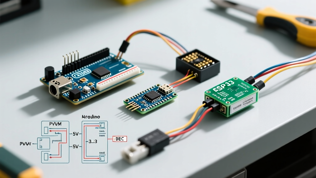
If you connect a 3.3V MCU (like the SAMD21 or ESP32) directly to a 5V-powered 74HC595, the 3.3V output falls dangerously close to the undefined region between V_IL (max 1.35V) and V_IH (min 3.15V). While it might work on a short breadboard wire at room temperature, thermal drift or slight voltage droops will cause missed bits.
The HCT Solution and Level Translation
To resolve this without adding bulky logic level shifters, swap the HC series for the HCT (High-speed CMOS, TTL-compatible) series, such as the NXP 74HCT595. The NXP 74HCT595 Datasheet specifies a V_IH of just 2.0V, regardless of whether VCC is 4.5V or 5.5V. This makes the 74HCT595 natively compatible with 3.3V MCU GPIO pins while still driving 5V outputs to downstream components.
If you must use a standard 74HC595 with a 3.3V MCU, you have two reliable hardware fixes:
- Power the 74HC595 at 3.3V: If your downstream loads (like LEDs or 3.3V relays) accept 3.3V, power the shift register directly from the MCU 3.3V rail. The V_IH threshold drops to ~2.1V, making 3.3V GPIO signals perfectly valid.
- Use a Bi-Directional Level Shifter: For mixed-voltage systems, route the Data and Clock lines through a TXS0108E or TXB0104 level translator module (typically costing around $2.50). Ensure you connect the OE (Output Enable) pin to VCCA to prevent high-impedance floating states during MCU boot.
MCU Architecture and the Parasitic Capacitance Problem
The Arduino shiftOut() Reference documents the function as a software-based SPI implementation. On a 16MHz ATmega328P, the GPIO toggling speed is relatively slow, yielding a clock frequency of roughly 80 kHz. This slow edge rate is forgiving of poor wiring and high parasitic capacitance.
However, modern MCUs like the ESP32-S3 (240MHz) or the RP2040 (133MHz) execute the shiftOut() loop significantly faster. The GPIO pins can toggle in nanoseconds, pushing the effective clock frequency into the low megahertz range. At these speeds, the physical wiring becomes a transmission line.
Clock Ringing and Double-Clocking
When using long jumper wires on a breadboard, the parasitic capacitance (often 2-5pF per inch) combined with the inductance of the wire creates an LC tank circuit. The ultra-fast rising edges from an RP2040 will cause severe 'ringing' (voltage oscillations) on the clock line. If the ringing dips below the V_IL threshold and crosses back above V_IH before the data line settles, the 74HC595 will register two clock pulses instead of one. This shifts your data out of alignment, resulting in scrambled LED patterns or relay chatter.
Actionable Fix: When using shiftOut() on ARM Cortex-M0+ or Xtensa LX6/LX7 MCUs, solder a 33-ohm to 47-ohm series resistor directly at the MCU clock output pin. This RC snubber dampens the high-frequency harmonics, rounding off the sharp square wave edges and eliminating clock ringing without violating the setup and hold times ($t_{su}$ and $t_{h}$) of the shift register.
Shift Register IC Compatibility Matrix
Not all shift registers are created equal. Below is a compatibility matrix detailing how different IC families interact with the shiftOut() function across varying logic domains.
| IC Family / Model | VCC Range | V_IH (Min @ 5V VCC) | 3.3V MCU Direct Drive? | Output Type | Best Use Case |
|---|---|---|---|---|---|
| SN74HC595N (TI) | 2V - 6V | 3.15V | No (Unreliable) | Push-Pull CMOS | 5V AVRs, Standard LED matrices |
| 74HCT595D (NXP) | 4.5V - 5.5V | 2.0V | Yes (Native) | Push-Pull CMOS | ESP32/RP2040 driving 5V loads |
| TPIC6B595N (TI) | 4.5V - 5.5V | 2.0V (TTL compat.) | Yes | Open-Drain (High Side) | 12V Relays, Solenoids, Automotive |
| CD4014B (TI) | 3V - 15V | ~3.5V @ 5V | No | Push-Pull CMOS | High-voltage industrial (12V VCC) |
High-Power Compatibility: The TPIC6B595 Open-Drain Architecture
When your project requires switching 12V solenoids, high-current LED strips, or automotive relays, the standard 74HC595 will fail; its push-pull outputs are limited to roughly 35mA per pin and 70mA total package current. For these scenarios, the TPIC6B595 is the industry standard.
The TPIC6B595 features open-drain DMOS outputs capable of sinking up to 150mA continuous current per channel at 50V. From a shiftOut() perspective, the serial interface is identical. However, the hardware wiring requires a crucial adjustment: because the outputs are open-drain (they can only pull to ground), you must wire your loads between the positive voltage rail (e.g., 12V) and the shift register output pins. Furthermore, you must place a flyback diode (like the 1N4148 or 1N4007) across inductive loads to prevent back-EMF from destroying the internal DMOS transistors when the channel switches off.
Critical Pin Handling: SRCLR and RCK
Software compatibility is only half the battle; improper hardware initialization of the shift register pins will cause boot-up glitches. The shiftOut() function only handles the SER (Serial Data), SRCLK (Shift Register Clock), and internally manages the timing. It does not manage the control pins.
- SRCLR (Shift Register Clear - Pin 10): This pin is active LOW. Many beginners leave this pin floating, which acts as an antenna for EMI and randomly clears the shift register. Rule: Always tie SRCLR directly to VCC if you do not need hardware clearing.
- RCK (Register Clock / Latch - Pin 12): This pin transfers the internal shift register data to the output storage register. It must be pulled LOW before calling
shiftOut(), and pulsed HIGH immediately after. If you are daisy-chaining multiple ICs, ensure the RCK pulse occurs only after all chainedshiftOut()commands have executed, otherwise the displays will visibly flicker during the shifting process.
Decoupling and Power Delivery Rules
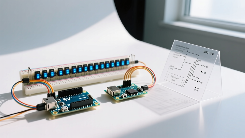
When daisy-chaining three or more shift registers to drive 24+ outputs, the instantaneous current draw during a state change (especially with capacitive loads like long LED strips) can cause localized VCC sags. This sag can drop the voltage below the brown-out threshold of the shift register, corrupting the internal logic state.
Hardware Mandate: Place a 0.1µF (100nF) X7R ceramic bypass capacitor across the VCC and GND pins of every single shift register IC, positioned as physically close to the IC pins as possible. For chains exceeding five ICs, add a bulk 10µF to 47µF electrolytic capacitor at the power entry point of the chain to handle low-frequency transient demands.
Troubleshooting Common shiftOut() Edge Cases
1. Data is Shifted by One Bit
Cause: Violation of the setup time ($t_{su}$). The data line is changing state while the clock line is transitioning.
Fix: Ensure your code sets the Data pin state before pulsing the Clock pin HIGH. The internal Arduino shiftOut() function handles this correctly, but if you wrote a custom bit-bang loop, verify the instruction order.
2. Random Outputs Flickering on Boot
Cause: The MCU GPIO pins are in a high-impedance (INPUT) state during the bootloader sequence before setup() runs.
Fix: Add 10k-ohm pull-down resistors on the RCK (Latch) pin to keep the outputs disabled until the MCU explicitly takes control and drives RCK HIGH.
3. Transitioning to Hardware SPI
If your project requires high-speed multiplexing (e.g., driving high-refresh-rate LED cubes), the software-based shiftOut() will bottleneck your MCU. In these cases, abandon shiftOut() and migrate to the hardware SPI.transfer() library. The hardware SPI peripheral handles the clock and data shifting via DMA (Direct Memory Access) on ARM MCUs, freeing the CPU and guaranteeing precise, jitter-free timing regardless of interrupt load.