
The Hidden Bottleneck in Hardware Prototyping
For professional makers and engineering students alike, the most frustrating delays in embedded systems development rarely stem from writing C++ code. Instead, the bottleneck is almost always hardware integration—specifically, the physical and electrical stacking of expansion boards. When you build a complex sensor node or robotic controller, an Arduino shield Uno configuration is the fastest way to prototype. However, haphazardly stacking a motor driver, an LCD display, and a wireless transceiver often leads to silent failures: I2C address collisions, SPI bus lockups, and severe voltage regulator thermal throttling.
In 2026, with the Arduino Uno R4 Minima and WiFi variants sitting alongside the legendary Uno Rev3 on workbenches worldwide, managing hardware workflows requires a disciplined approach. This guide details a rigorous workflow optimization strategy for stacking Uno shields, focusing on pin auditing, power budgeting, mechanical clearance, and non-destructive debugging.
Pre-Stack Audit: The Pin Conflict Matrix
Before a single shield is pressed onto the female headers, you must conduct a paper or digital pin audit. The Uno form factor exposes 14 digital I/O pins and 6 analog inputs, but standard communication protocols consume these in rigid blocks. Overlooking this leads to the most common prototyping failure: two shields attempting to drive the same pin simultaneously, which can permanently damage the ATmega328P or Renesas RA4M1 microcontroller.
| Uno Pin(s) | Protocol | Common Shield Usage | Collision Risk & Workflow Mitigation |
|---|---|---|---|
| D11, D12, D13 | SPI (MOSI, MISO, SCK) | SD Cards, Ethernet, TFT Displays | High. Shared bus. Mitigate by routing individual Chip Select (CS) pins to unused D2-D9. |
| A4, A5 | I2C (SDA, SCL) | OLEDs, IMUs, Motor Controllers | Medium. Bus is shared, but addresses collide. Use I2C multiplexers (e.g., TCA9548A) if shields share hardcoded addresses. |
| D0, D1 | UART (RX, TX) | GPS, Cellular, Bluetooth | Critical. Conflicts with USB serial debugging. Use SoftwareSerial on D2/D3 for secondary shields. |
| D3, D5, D6, D9, D10, D11 | PWM | Servos, LED Drivers, Motor PWM | High. Often overlaps with SPI (D11). Reassign PWM functions via timer registers if possible. |
Resolving Protocol Collisions in Modern Workflows
When your project demands multiple shields that utilize the same communication bus, you must implement logical separation in your workflow.
SPI Chip Select (CS) Management
The SPI bus is a shared highway, but each device needs a unique tollbooth. According to the official Arduino SPI documentation, the hardware SS pin (D10 on the Uno) must be kept as an output to maintain SPI master mode. However, when stacking an Ethernet shield and an SD card shield, both default to using D10 or D4 for CS.
Workflow Optimization: Physically bend the CS pin header on the top shield so it does not insert into the bottom shield's D4 hole. Instead, use a jumper wire to route that CS pin to an unused digital pin (e.g., D7), and update your sketch's pinMode(7, OUTPUT) initialization accordingly.
I2C Address Translation
I2C is elegant until you stack two shields featuring the PCF8574 I/O expander—commonly found on 16x2 LCD backpacks and relay modules—both hardcoded to address 0x27.
Workflow Optimization: Rather than desoldering surface-mount address pads on the shield, integrate a TCA9548A I2C multiplexer breakout board between the Uno and the conflicting shields. This allows your microcontroller to switch I2C channels on the fly, effectively isolating the shields and eliminating address collisions without altering the shield hardware.
Power Rail Budgeting: Avoiding Thermal Shutdown
The most insidious failure mode in an Arduino shield Uno stack is power starvation. Makers frequently assume that because a shield physically fits, the Uno can power it. This is dangerously incorrect, particularly when using the onboard linear voltage regulator.
Engineering Warning: The classic Arduino Uno Rev3 utilizes an NCP1117ST50T3G 5V linear regulator. If you power the Uno via the barrel jack with a 9V adapter and draw 400mA through a stacked servo shield, the regulator must dissipate 1.6 Watts of heat ((9V - 5V) * 0.4A). The SOT-223 package will exceed its 150°C thermal shutdown threshold in under 45 seconds without active cooling.
The Power Budgeting Workflow:
- Calculate Total 5V Draw: Sum the maximum current draw of all stacked shields. An Adafruit Motor Shield V2 drawing 1.5A for steppers will instantly fry the Uno's USB polyfuse (rated at 500mA) or the barrel jack regulator.
- Inject Power Directly: For high-current stacks, bypass the Uno's regulator entirely. Use a shield with a dedicated terminal block (like the Adafruit Motor Shield V2) and wire your 5V/12V external power supply directly into the shield's VIN or dedicated power terminals.
- Verify 3.3V Limits: If you are using an Uno R4 WiFi, the 3.3V rail can supply up to 500mA, which is excellent for modern ESP32-based wireless shields. The older Rev3, however, relies on the onboard ATmega16U2's 3.3V regulator, which is capped at a mere 50mA. Stacking a 3.3V LoRa shield on a Rev3 without an external buck converter will result in brownouts and corrupted transmissions.
Mechanical Clearance: The 11mm vs 15mm Header Rule
A physical workflow bottleneck occurs when a shield's PCB shorts against the Uno's USB Type-B port or DC barrel jack. Standard female headers are typically 8.5mm to 11mm tall. The metal casing of the USB-B port on the Uno Rev3 stands at roughly 10.5mm. If you stack a shield with exposed solder joints or a flat ground plane on the bottom using standard 11mm headers, you risk a dead short against the USB casing.
Workflow Optimization: Standardize your prototyping inventory to use 15mm stacking headers for the first layer above the Uno. This provides a 4.5mm clearance margin, ensuring that bulky components like RJ45 magjacks (on Ethernet shields) or SD card cages do not mechanically foul the Uno's ports. For subsequent shield layers, standard 11mm headers are perfectly safe, as the PCB below them provides flat clearance.
Debugging Stacked Shields Without Tear-Downs
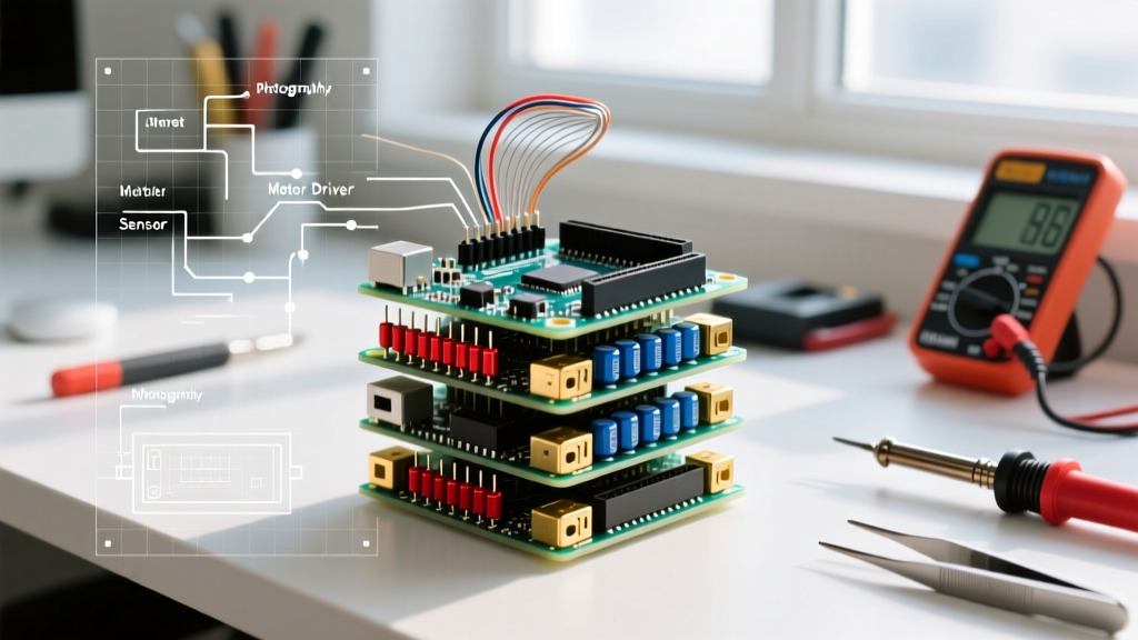
Once your Arduino shield Uno stack is assembled, probing test points with a multimeter or logic analyzer becomes a physical nightmare. The top shield obscures the test pads of the bottom shield, forcing you to repeatedly disassemble the stack to debug—a massive waste of time.
The Z-Axis Debugging Strategy
To optimize your debugging workflow, integrate a Z-axis expansion breakout board or a prototyping shield with extended lateral bus strips at the very bottom of your stack (directly on top of the Uno).
- Route I2C/SPI laterally: Before stacking the second shield, solder lateral pin headers to the SDA, SCL, MOSI, and MISO lines on your base proto-shield. This gives you easy access to clip on a Saleae logic analyzer without dismantling the stack.
- Use Serial Pass-Through: If debugging a GPS or cellular shield buried in the middle of a stack, utilize a dedicated debug firmware that echoes the shield's UART data to the Uno's primary Serial port (D0/D1), allowing you to monitor raw NMEA or AT commands via the USB serial monitor.
- Thermal Imaging: Keep a basic thermal camera (like the FLIR ONE or InfiRay P2) at your bench. When a stacked shield experiences a silent I2C lockup or a shorted MOSFET, a quick thermal sweep will instantly reveal the offending component glowing at 80°C+ without requiring you to unplug a single header.
Conclusion
Treating an Arduino shield Uno stack as a simple plug-and-play toy is a recipe for fractured workflows and damaged silicon. By adopting a rigorous pre-stack pin audit, respecting the thermal limits of linear regulators, enforcing 15mm mechanical clearances, and planning for Z-axis debugging, you transform the Uno from a basic learning tool into a robust, rapidly deployable prototyping platform. For the deepest hardware specifications and schematic references, always consult the official Arduino hardware documentation before finalizing your shield stack architecture.