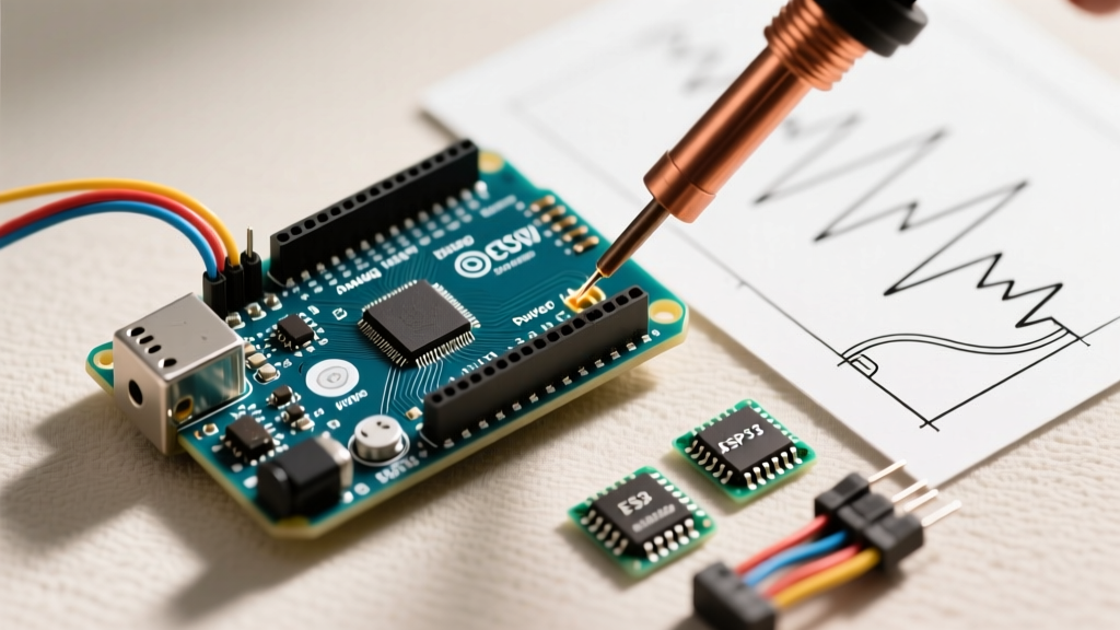

Understanding the ATmega328P Architecture
When configuring a new microcontroller project, mastering the arduino pinout uno is the foundational step that separates reliable deployments from frustrating hardware failures. The classic Arduino Uno R3, powered by the Microchip (formerly Atmel) ATmega328P-PU microcontroller, remains the industry standard for prototyping in 2026. While newer boards like the Uno R4 Minima have entered the market, the R3's 8-bit AVR architecture dictates specific electrical behaviors, current limitations, and memory mappings that every maker must understand.
According to the official Arduino Uno Rev3 documentation, the board features 14 digital input/output pins, 6 analog inputs, a 16 MHz quartz crystal, and a USB Type-B connection. However, the physical silkscreen on the PCB only tells half the story. True configuration expertise requires understanding the underlying electrical tolerances, pulse-width modulation (PWM) frequencies, and thermal limits of the onboard voltage regulators.
Digital I/O Pins: Configuration and PWM Mapping
The Uno provides 14 digital pins (D0 to D13). Each pin can be configured as an INPUT, OUTPUT, or INPUT_PULLUP using the standard Arduino IDE functions. However, treating all digital pins as identical is a common configuration error.
Internal Pull-Up Resistors
When configuring a pin as INPUT_PULLUP, the microcontroller engages an internal resistor tied to the 5V rail. The ATmega328P datasheet specifies this resistance is not a fixed value; it varies between 20kΩ and 50kΩ depending on the specific silicon batch and operating temperature. For precision timing circuits or high-impedance sensor arrays, relying on internal pull-ups can introduce jitter. In these scenarios, configuring the pin as standard INPUT and adding an external 10kΩ metal-film resistor is the professional standard.
PWM Frequencies and Timer Conflicts
Six of the digital pins (3, 5, 6, 9, 10, and 11) support hardware PWM, denoted by the tilde (~) symbol. While the analogWrite() function defaults to an 8-bit resolution (0-255), the underlying hardware timers dictate the actual output frequency:
- Pins 5 and 6: Driven by Timer0, which operates at 980 Hz. Note that altering Timer0 affects the
millis()anddelay()functions. - Pins 9 and 10: Driven by Timer1, operating at 490 Hz. Timer1 is a 16-bit timer, allowing for higher resolution PWM if you bypass the standard Arduino core libraries and write directly to the registers.
- Pins 3 and 11: Driven by Timer2, operating at 490 Hz.
As detailed in the Arduino Digital Pins Foundation Guide, configuring these pins requires careful planning if your sketch utilizes third-party libraries that hijack specific hardware timers for interrupt service routines (ISRs).
Analog Inputs: ADC Resolution and Voltage Reference
Pins A0 through A5 are mapped to the microcontroller's internal 10-bit Analog-to-Digital Converter (ADC). This provides a resolution of 1024 discrete steps. With the default 5V reference, each step represents approximately 4.88 mV.
Source Impedance and Sampling Errors
A critical, often overlooked aspect of analog configuration is the source impedance of the sensor being read. The ATmega328P ADC utilizes an internal sample-and-hold capacitor (approximately 14 pF). If the external circuit has a high output impedance (greater than 10kΩ), the internal capacitor cannot charge fully within the 1.5 ADC clock cycle sampling window. This results in artificially low and noisy readings. To configure high-impedance sensors like thermistors or photoresistors correctly, you must either buffer the signal with an op-amp or add a 100nF ceramic capacitor between the analog pin and ground to act as a local charge reservoir.
Adjusting the Voltage Reference
For sensors that output a maximum of 3.3V, using the 5V rail wastes nearly 35% of your ADC resolution. You can reconfigure the reference voltage using analogReference(EXTERNAL) and feeding a clean 3.3V signal into the AREF pin. Never connect a voltage higher than 5V to the AREF pin, as this will permanently destroy the ADC multiplexer.
Power Distribution and Thermal Limitations
Power configuration is where most hardware damage occurs. The Uno features multiple power access points, but they are not created equal. The board utilizes an NCP1117ST50T3G (or equivalent) linear voltage regulator to drop voltage from the VIN pin or the barrel jack down to 5V.
| Pin / Source | Voltage | Max Recommended Current | Notes & Thermal Constraints |
|---|---|---|---|
| 5V Pin | 5.0V | 500mA (via USB) | Bypasses the onboard regulator. Limited by the host PC USB port or external 5V supply. |
| 3.3V Pin | 3.3V | 150mA | Generated by the onboard LP2985 regulator on the USB interface chip. Do not exceed. |
| VIN / Barrel Jack | 7V - 12V | 1A (Absolute Max) | Subject to severe thermal throttling. See thermal dissipation notes below. |
| IOREF | 5.0V | Signal Only | Provides a reference voltage for shields to configure their logic levels. |
The Linear Regulator Thermal Trap
Linear regulators dissipate excess voltage as heat. If you supply 12V to the VIN pin and draw 300mA from the 5V pin, the regulator must drop 7V at 0.3A. This equates to 2.1 Watts of thermal dissipation. The SOT-223 package on the Uno PCB lacks a dedicated heatsink and will trigger its internal thermal shutdown protection (typically around 150°C junction temperature) within minutes. For projects requiring more than 200mA at 5V, configure your power delivery using an external switching buck converter (like an LM2596 module) wired directly to the 5V pin, completely bypassing the inefficient onboard linear regulator.
Communication Protocols: UART, SPI, and I2C Pin Mapping
Proper bus configuration prevents data corruption and I2C lockups.
- UART (Serial): Pins D0 (RX) and D1 (TX). These are routed through the secondary ATmega16U2 USB-to-Serial chip. If you are uploading a sketch that heavily utilizes
Serial.print()during thesetup()phase, you may experience upload timeouts. Always disconnect external hardware from D0 and D1 during firmware flashing. - SPI: Pins D11 (MOSI), D12 (MISO), D13 (SCK), and D10 (SS). The Uno also breaks these out to the 2x3 ICSP header. Configuring multiple SPI devices requires individual chip select (SS) lines for each peripheral; the hardware MISO/MOSI/SCK lines must remain shared in parallel.
- I2C (Wire): Pins A4 (SDA) and A5 (SCL). The ATmega328P does not have internal I2C pull-up resistors. While many modern sensor modules include 4.7kΩ pull-ups on their breakout boards, chaining more than three I2C devices often degrades the signal rise time. In complex configurations, adding a dedicated I2C level-shifter or external 2.2kΩ pull-up resistors to the 5V rail is mandatory for bus stability.
Common Configuration Mistakes and Hardware Failure Modes
Even experienced engineers fry boards by ignoring the electrical realities of the arduino pinout uno. Here are the most common fatal configuration errors:
The Backfeed Disaster: Supplying 5V to the 5V pin while simultaneously having a 9V battery connected to the VIN pin or barrel jack. This forces current backward through the linear regulator, destroying it instantly. Always use a DPDT switch or diode OR-ing when managing dual power sources.
Exceeding the VCC Current Limit
While a single I/O pin can source or sink up to 20mA (with an absolute maximum rating of 40mA), the microcontroller has a total package current limit of 200mA across all VCC and GND pins combined. Configuring 14 digital pins to drive standard 20mA LEDs simultaneously will draw 280mA, exceeding the silicon limits and causing the ATmega328P to brownout or permanently latch up. Always use N-channel MOSFETs (like the 2N7000) or ULN2803 Darlington arrays to drive high-current loads.
Inductive Kickback on Relay Pins
Connecting a 5V relay coil directly to a digital pin without a flyback diode. When the pin goes LOW, the collapsing magnetic field in the relay coil generates a high-voltage spike (often exceeding 30V) that travels back into the microcontroller's I/O buffer, destroying the pin's internal ESD protection diodes. Always configure a 1N4148 diode in reverse bias across any inductive load.
Frequently Asked Questions (FAQ)
Can I power the Uno via the 5V pin and USB simultaneously?
Yes, but with caveats. The Uno features a hardware comparator circuit (built around an LMV358 op-amp) that controls a P-channel MOSFET to automatically switch between USB power and the onboard 5V regulator. However, if you inject 5V into the 5V pin while the USB is connected, you are bypassing the auto-selection circuit and directly tying your external 5V source to the host PC's USB 5V rail. This can cause ground loops or backfeed into your computer. It is safer to cut the VUSB jumper pad on the underside of the PCB if you intend to permanently power the board via the 5V pin.
What is the actual cost of a genuine Uno in 2026?
As of 2026, a genuine Arduino Uno R3 purchased directly from the official Arduino Store retails for approximately $27.00 to $29.00 USD. High-quality third-party clones (such as those from Elegoo or HiLetgo) utilizing the CH340 USB-to-Serial chip instead of the ATmega16U2 can be found for $12.00 to $15.00 USD. While clones are fine for basic breadboarding, genuine boards offer superior USB stability and stricter quality control on the 16MHz crystal oscillators, which is vital for precise UART baud rate generation.