
The Evolution of the Standard Uno Header
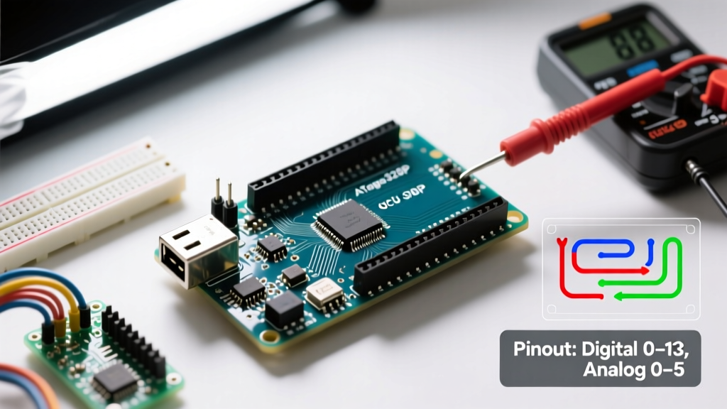
When discussing the pin configuration of Arduino Uno, most makers immediately picture the classic 14 digital and 6 analog headers that have defined embedded prototyping for over a decade. However, as of 2026, the landscape has shifted. The introduction of the Uno R4 Minima and Uno R4 WiFi fundamentally altered the logical capabilities hidden beneath the familiar physical footprint. While the physical header spacing remains identical to ensure backward compatibility with legacy shields, the electrical characteristics, current limits, and peripheral routing have undergone a massive overhaul.
In this comprehensive board review and comparison, we dissect the exact pinout differences between the legacy ATmega328P-based Uno R3 and the modern Renesas RA4M1-based R4 variants. Whether you are designing a custom PCB shield, wiring high-current relays, or integrating 3.3V I2C sensors, understanding these hardware-level nuances is critical to avoiding catastrophic component failure.
Logical Pin Configuration of Arduino Uno: R3 vs R4 Matrix
Before wiring your next project, review this hardware-level comparison matrix. The shift from an 8-bit AVR architecture to a 32-bit ARM Cortex-M4 brings significant changes to how the pins behave under load.
| Feature / Specification | Uno R3 (ATmega328P) | Uno R4 Minima (RA4M1) | Uno R4 WiFi (RA4M1 + ESP32-S3) |
|---|---|---|---|
| Core Architecture | 8-bit AVR @ 16 MHz | 32-bit ARM Cortex-M4 @ 48 MHz | 32-bit ARM @ 48 MHz + ESP32-S3 |
| Digital I/O Pins | 14 (D0 - D13) | 14 (D0 - D13) | 14 (D0 - D13) |
| PWM Capable Pins | 6 (D3, 5, 6, 9, 10, 11) | 6 (D3, 5, 6, 9, 10, 11) | 6 (D3, 5, 6, 9, 10, 11) |
| Analog Inputs (ADC) | 6 (10-bit resolution) | 6 (14-bit resolution) | 6 (14-bit resolution) |
| True Analog Output (DAC) | None (PWM only) | 1 (A0) | 1 (A0) |
| Max DC Current per I/O | 20 mA (Absolute max 40 mA) | 8 mA (Absolute max 20 mA) | 8 mA (Absolute max 20 mA) |
| Native Logic Level | 5V | 5V (with 3.3V tolerant inputs) | 5V (with 3.3V tolerant inputs) |
Source: Official Arduino Uno R3 Documentation and Arduino Uno R4 Minima Documentation.
Power Rail Architecture & Edge Cases
The power pins on the Uno are notoriously misunderstood, leading to thousands of fried boards and unstable sensor readings every year. The physical pins include 5V, 3.3V, GND, Vin, and IOREF. Here is how they actually behave across the generations.
The 3.3V Regulator Trap
On the classic Uno R3, the 3.3V pin is fed by an onboard LP2985 voltage regulator that is thermally limited to roughly 50 mA. If you attempt to power a modern ESP8266 module or a high-draw TFT display directly from the R3's 3.3V pin, the regulator will overheat, drop voltage, and potentially trigger thermal shutdown. In contrast, the Uno R4 series utilizes a more robust power management IC (PMIC) that can comfortably supply up to 300 mA on the 3.3V rail, making it vastly superior for modern sensor arrays.
Vin vs. 5V: The Diode Drop Reality
A common failure mode occurs when makers backfeed power. If you supply 5V through the Vin pin, the voltage must pass through a reverse-polarity protection diode (typically an M7 or SS34). This introduces a voltage drop of roughly 0.6V to 0.7V, meaning your board will only receive ~4.3V, causing brownouts. Rule of thumb: If you are injecting regulated 5V from an external buck converter, always use the 5V pin directly, bypassing the diode and the onboard linear regulator entirely.
IOREF: The Shield Handshake
The IOREF pin outputs the operating voltage of the microcontroller (5V on all standard Unos). Smart shields read this pin to configure their own logic level shifters. Never hardwire IOREF to a voltage source; it is strictly an output reference pin.
Digital, Analog, and Communication Pin Nuances
While the silkscreen labels remain identical, the internal routing of the Renesas RA4M1 on the R4 boards introduces new capabilities and restrictions.
The DAC Advantage on Pin A0
On the Uno R3, generating an analog voltage requires using analogWrite() on a PWM pin, which outputs a high-frequency square wave that must be filtered with an external RC low-pass circuit. The Uno R4 Minima and WiFi feature a true 12-bit Digital-to-Analog Converter (DAC) hardwired to pin A0. By using analogWrite(A0, value) on the R4, you get a genuine, stable DC voltage output without external capacitors—a massive advantage for audio synthesis and precision control loops.
I2C and SPI Routing
- I2C (SDA/SCL): On the R3, SDA and SCL are internally duplicated to pins A4 and A5. The R4 maintains this physical duplication but routes them through the RA4M1's dedicated I2C peripheral, supporting faster bus speeds (up to 1 MHz Fast Mode Plus).
- SPI (MOSI/MISO/SCK): Pins 11, 12, and 13 serve as the primary SPI bus. On the R4 WiFi, the ESP32-S3 co-processor shares the board space, but the primary SPI header remains dedicated to the RA4M1 to prevent bus contention with shields.
- UART (TX/RX): Pins 0 and 1 are tied to the primary hardware serial port. On the R4 WiFi, debugging and serial routing are more complex due to the ESP32 bridge; users must ensure they are not conflicting with the internal UART bridge when using pins 0 and 1 for external GPS or cellular modules.
Shield Compatibility & The 3.3V Sensor Trap
The physical pin configuration of the Arduino Uno was designed in an era when 5V logic was the standard. Today, 90% of new sensors (BME280, VL53L0X, modern OLEDs) operate strictly at 3.3V and are not 5V tolerant.
⚠️ Critical Warning: The 5V I2C DestroyerIf you connect a 3.3V I2C sensor directly to the Uno R3's A4/A5 pins, the ATmega328P will push 5V logic high into the sensor's SDA line. This will instantly fry the sensor's internal pull-up resistors or ESD protection diodes. While the Uno R4's RA4M1 inputs are 5V tolerant, its I2C lines still pull up to 5V via the board's internal routing when configured for legacy compatibility. Always use a bidirectional logic level shifter (like the BSS138-based Adafruit 757) when interfacing 3.3V sensors with any 5V Uno variant.
Expert FAQ: Common Pin Configuration Questions
Can I draw 40mA from a single digital pin on the Uno R3?
While the ATmega328P datasheet lists an absolute maximum rating of 40mA per I/O pin, operating continuously at this limit causes excessive internal heating and voltage sag. For reliable 2026 designs, limit continuous draw to 20mA per pin, and ensure the total combined current across all Port B, C, and D pins does not exceed the package limit of 200mA. Use a logic-level MOSFET (like the IRLZ44N) for anything higher.
Why does my Uno R4 read different analog values than my R3?
The Uno R3 uses a 10-bit ADC (values 0-1023). The Uno R4 features a 14-bit ADC. However, the Arduino IDE's analogRead() function defaults to returning a 10-bit resolution for backward compatibility. To unlock the R4's true 14-bit precision (values 0-16383), you must explicitly call analogReadResolution(14) in your setup loop.
Are the ICSP headers identical across all versions?
Yes, the 2x3 ICSP header remains physically and electrically consistent in its placement. However, on the R4 boards, the ICSP header routes directly to the RA4M1's SWD (Serial Wire Debug) and SPI pins, allowing for hardware debugging via an ST-Link or J-Link probe—a feature entirely absent on the legacy R3.
Pro-Tip for Custom Shield Design: When designing a PCB shield that mates with the Uno header, always place a 100nF decoupling capacitor as close to the5VandGNDentry points of your shield as possible. The long physical traces of the Uno's female headers introduce parasitic inductance, which can cause high-frequency noise when switching relays or driving LED matrices.