
The Global Component Challenge: Decoding the Tranzistor PNP
When sourcing components from international surplus markets, reading legacy Eastern European schematics, or ordering from global distributors, you will frequently encounter the term tranzistor PNP. While "tranzistor" is simply the Romanian, Czech, or Slovak translation for transistor, identifying these specific PNP (Positive-Negative-Positive) bipolar junction transistors (BJTs) requires a solid grasp of universal semiconductor physics, package pinouts, and multimeter testing. Whether you are holding a standard BC327 or a rugged KT818 power transistor, proper identification is the first line of defense against circuit failure.
In this component identification guide, we will bypass the basic theory and dive straight into the practical, actionable methods for verifying PNP transistors. We will cover visual package inspection, the definitive multimeter diode test, and how to cross-reference regional marking schemes to ensure your prototyping and repair projects succeed.
Visual Identification: Package Codes and Markings
The physical package of a tranzistor PNP dictates its thermal dissipation capabilities and, crucially, its pinout configuration. However, visual identification is fraught with pitfalls, especially when dealing with international equivalents or New Old Stock (NOS) components.
TO-92 Through-Hole Packages
The TO-92 is the most common package for small-signal PNP transistors like the 2N3906 or BC327. When looking at the flat side of the transistor with the pins pointing downward, the standard Western pinout is Emitter-Base-Collector (EBC). However, many Asian-manufactured equivalents and older Eastern European 'tranzistor' variants utilize a Collector-Base-Emitter (CBE) or Emitter-Collector-Base (ECB) configuration. Never assume the pinout based solely on the package shape.
TO-220 Power Packages
For power switching applications, the TO-220 package (e.g., TIP32C) is ubiquitous. The metal tab is almost universally connected to the Collector to facilitate heatsink mounting. Because the Collector is tied to the tab, you can easily identify it by testing for continuity between the tab and the pins. The standard pinout for TO-220 PNP transistors is Base-Collector-Emitter (BCE), but verifying with a multimeter remains mandatory.
The SOT-23 Surface Mount Trap
Surface mount PNP transistors like the MMBT3906 use the SOT-23 package. These are marked with cryptic 2- or 3-character codes (e.g., "3E" or "K2") rather than full part numbers. Identifying these requires a SMD code book or datasheet cross-reference. Furthermore, the pinout is typically Base-Emitter-Collector (BEC), but the physical orientation on the PCB pad can easily be misinterpreted during rework.
The Multimeter Diode Test: Definitive Pinout Verification
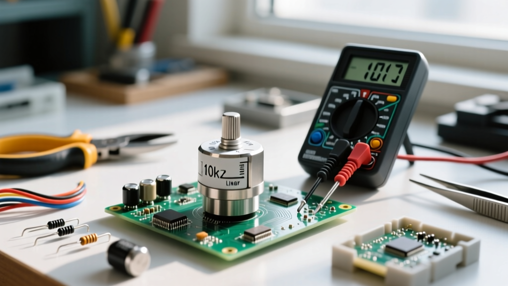
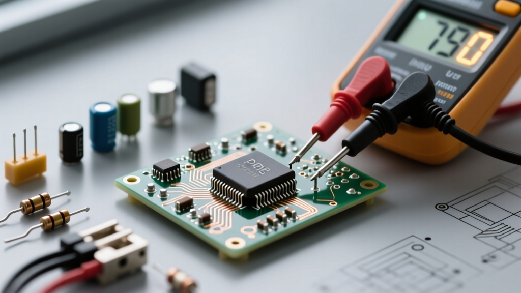
Visual markings can be faked, sanded off, or misprinted. The only 100% reliable method to identify a tranzistor PNP and its pinout is using the Diode Test mode on a digital multimeter (DMM). This method exploits the internal PN junctions of the BJT.
Expert Insight: A PNP transistor is essentially two PN junction diodes sharing a common N-type Base. To forward-bias these junctions, your multimeter's internal battery must apply negative voltage to the Base. Therefore, the Black probe (negative) must go to the Base, and the Red probe (positive) to the Emitter and Collector. This is the exact opposite of NPN testing.
Step-by-Step PNP Verification Protocol
- Set the DMM: Switch your multimeter to the Diode Test mode (usually indicated by a diode symbol).
- Find the Base: Place the Black probe on any pin. Touch the Red probe to the other two pins. If you get a forward voltage drop reading (typically 0.600V to 0.750V for Silicon, or 0.200V to 0.300V for Germanium) on both pins, the pin under the Black probe is the Base.
- Confirm PNP Polarity: If the Black probe is on the Base and yields forward readings, it is definitively a PNP transistor. (If the Red probe on the Base yielded the readings, it would be NPN).
- Identify Emitter vs. Collector: The Emitter is heavily doped compared to the Collector. Therefore, the forward voltage drop between Base and Emitter will be slightly higher (by about 5mV to 15mV) than the Base-Collector junction. Note the two readings; the pin giving the slightly higher voltage drop is the Emitter.
Cross-Reference Matrix: Standard vs. Regional Equivalents
When repairing imported electronics or building from international schematics, you may need to substitute a standard Western PNP with a regional 'tranzistor' equivalent. Below is a cross-reference table for common PNP substitutions.
| Western Standard | Regional / Tranzistor Equivalent | Package | Max Ic (A) | Vce(sat) Typical |
|---|---|---|---|---|
| BC327 | BC328 / KT3107 (Legacy) | TO-92 | 0.8 | -0.3V |
| 2N3906 | KT361 / BC212 | TO-92 | 0.2 | -0.25V |
| TIP32C | KT818 / BD912 | TO-220 | 3.0 | -1.2V |
| 2N2907 | KT3108 / BC557 | TO-92 | 0.6 | -0.4V |
For deeper theoretical understanding of how these junctions operate under load, refer to the comprehensive Bipolar Transistor tutorials on Electronics Tutorials, which detail the doping concentrations that cause the Vce(sat) variations seen above.
Spotting Counterfeits and Degraded Silicon
The secondary market is flooded with counterfeit transistors. A common scam involves taking cheap, low-current NPN transistors, sanding off the markings, and reprinting them as high-value PNP power transistors. Here is how to spot them:
The Acetone and Scratch Test
Genuine semiconductor manufacturers use hardened epoxy and laser etching or deep ink stamping. Counterfeiters often use a cheap black paint over sanded markings. Rub the top of the tranzistor PNP with a cotton swab soaked in acetone or isopropyl alcohol. If the black residue comes off, or if the text smears, it is a counterfeit. Additionally, run your fingernail over the text; genuine laser etching will feel perfectly smooth or uniformly indented, while fake silk-screening will feel raised.
Thermal Fatigue and Micro-Cracks
When salvaging PNP transistors from old PCBs, excessive heat from desoldering can cause internal die detach or micro-cracks in the epoxy. A transistor that passes the multimeter diode test at room temperature might fail under load due to thermal runaway. As the junction temperature rises, the leakage current (Icbo) increases. In a compromised die, this creates a positive feedback loop, leading to secondary breakdown. Always test salvaged TO-220 PNP transistors by applying a moderate load and monitoring the case temperature with a thermal camera or thermocouple. For more on safely testing and switching transistors, consult the SparkFun Transistor Guide.
Summary: Best Practices for the Workbench
Identifying a tranzistor PNP goes far beyond reading the text printed on the epoxy. By combining visual package inspection, rigorous multimeter diode testing, and an understanding of regional cross-references, you eliminate the guesswork from your electronics prototyping. Always keep a dedicated component tester or a reliable DMM on your bench, verify the Base-Emitter-Collector pinout before applying power, and remain highly skeptical of unbranded or suspiciously cheap power transistors. Mastering these identification skills will save you hours of debugging and protect your circuits from catastrophic failure.