When debugging a noisy PCB or a failing high-speed data link, many hobbyists and junior engineers throw ferrite beads at the problem and hope for the best. But true signal integrity troubleshooting requires a precise understanding of reactance vs impedance. Reactance is the frequency-dependent opposition to alternating current caused by energy storage in capacitors and inductors. Impedance is the total, complex opposition to current flow, combining both resistance (energy dissipation) and reactance (energy storage). In the context of noise control, confusing the two leads to misdiagnosed coupling paths and ineffective fixes.
The Core Difference: Reactance vs Impedance in Signal Paths
To diagnose noise, you must first separate the real and imaginary parts of your circuit's opposition to current. Resistance ($R$) dissipates energy as heat and is largely frequency-independent. Reactance ($X$) stores and releases energy, causing phase shifts and ringing, and varies wildly with frequency.
- Inductive Reactance ($X_L$): $X_L = 2\pi fL$. Increases with frequency. A 10nH via has an $X_L$ of 6.28 $\Omega$ at 100MHz, but 62.8 $\Omega$ at 1GHz.
- Capacitive Reactance ($X_C$): $X_C = 1 / (2\pi fC)$. Decreases with frequency. A 2pF stray capacitance between traces has an $X_C$ of 795 $\Omega$ at 100MHz, dropping to 79.5 $\Omega$ at 1GHz.
Impedance ($Z$) is the vector sum of both: $Z = R + jX$. The magnitude is $|Z| = \sqrt{R^2 + X^2}$. According to All About Circuits, while resistance dictates DC voltage drops, it is the reactance component of impedance that dictates high-frequency signal reflections, ringing, and susceptibility to noise coupling.
A high-impedance node (e.g., a 10k$\Omega$ pull-up on an I2C line) acts as an excellent antenna for electric fields (capacitive coupling). A low-impedance loop (e.g., a power ground return) acts as an excellent antenna for magnetic fields (inductive coupling). Identifying which impedance state your victim circuit is in tells you exactly which coupling path is attacking it.
Identifying the Dominant Coupling Path
When noise appears on your scope, your first question must be: which coupling path is dominant here? Noise transfers from an aggressor to a victim via three primary mechanisms. Identifying the correct one prevents you from applying the wrong fix.
1. Capacitive Coupling (Electric Fields)
Dominant when: The victim node has high impedance and the aggressor has high $dV/dt$ (fast voltage edges, like a switching clock). Stray mutual capacitance ($C_m$) forms a voltage divider with the victim's impedance to ground. If the victim's impedance is higher than the capacitive reactance ($X_C$) of the stray coupling path, massive noise injects into the node.
2. Inductive / Radiated Coupling (Magnetic Fields)
Dominant when: The victim forms a low-impedance loop and the aggressor has high $di/dt$ (fast current changes, like a switching buck converter or motor driver). Mutual inductance ($M$) induces a voltage ($V = M \cdot di/dt$) directly into the victim loop. The larger the physical loop area of the victim, the worse the coupling.
3. Conductive Coupling (Shared Impedance)
Dominant when: Two circuits share a physical return path (like a thin ground trace) that has non-zero impedance. When the aggressor draws a transient current, the voltage drop across the shared ground impedance ($V = I \cdot Z_{ground}$) appears directly in series with the victim's ground reference. This is commonly known as ground bounce.
Noise Mitigation Fixes Ranked by Cost and Effectiveness
Once you identify the coupling path, apply fixes based on physics, not guesswork. Below is a decision-tree-table ranking solutions by cost and effectiveness.
The cheapest fix that actually works: For inductive coupling, twisting your cable pairs or minimizing the PCB return loop area costs exactly $0.00 in layout changes and provides up to 40dB of common-mode rejection. For capacitive coupling, inserting a grounded guard trace between the aggressor and victim costs $0.00 and shunts the electric field to ground before it reaches the victim.
| Coupling Path | Primary Fix | Cost | Effectiveness | Engineering Notes |
|---|---|---|---|---|
| Inductive (Magnetic) | Minimize loop area / Twisted Pair | $0 - $2 | Extremely High | Twisting cancels magnetic flux. Keep signal and return paths tightly adjacent on PCBs. |
| Capacitive (Electric) | Guard traces / Lower victim impedance | $0 | High | Route a grounded trace between aggressor and victim. Lowering victim $Z$ (e.g., 50$\Omega$ termination) reduces the voltage divider effect. |
| Conductive (Shared Z) | Star grounding / Solid ground plane | $0 | High | Never route sensitive analog returns through digital ground paths. Use a continuous copper pour to minimize $Z_{ground}$. |
| Radiated (Far-field) | Metallic Shielding | $$$ | High (if done right) | Only effective if terminated correctly. See warning below. |
Never apply shielding without strict ground-termination rules. A shield is only as good as its termination. If you terminate a coaxial shield with a 'pigtail' wire, the inductive reactance of that wire at high frequencies ($X_L = 2\pi fL$) turns the shield itself into a radiating antenna. Shields must be terminated 360-degrees to the chassis or ground plane using a low-impedance bond.
Furthermore, avoid treating ferrite beads as a universal cure. Ferrite beads only add resistive loss at specific high-frequency resonant points. They do absolutely nothing to stop low-frequency magnetic coupling or ground bounce, and they can cause severe voltage droop if placed on a power rail with high transient current demands.
Proving the Fix: Before and After Measurement Methods
How do you prove the fix with a meter or scope? You cannot rely on 'it looks cleaner on the screen.' You need quantitative before-and-after data. Here is the step-by-step measurement protocol used on the bench.
- Baseline Impedance Profiling (TDR): To measure the actual impedance of a trace or cable, use Time Domain Reflectometry (TDR). Connect a TDR-equipped oscilloscope or sampling head to the line. The scope sends a fast step edge (e.g., 35ps rise time) and measures reflections. A flat 50$\Omega$ line indicates good integrity; spikes indicate vias or connectors where inductive reactance is causing impedance discontinuities.
- Baseline Noise Capture (FFT & Probes): Power the board. Use a near-field H-field probe (for magnetic loops) or E-field probe (for electric fields) connected to your oscilloscope. Capture the noise floor using the scope's FFT (Fast Fourier Transform) math function. Note the exact frequency bins and dBm amplitude of the noise peaks.
- Apply the Mitigation: Implement your fix (e.g., add the guard trace, twist the cable, or re-route the ground return).
- Verify the Delta: Re-measure with the exact same probe placement, scope attenuation, and FFT window settings. A successful fix will show a minimum 10dB to 20dB reduction in the specific frequency bins associated with the aggressor's switching harmonic.
FAQ: Reactance vs Impedance in High-Speed and Noisy Circuits
Why does high reactance cause more capacitive noise coupling than high resistance?
Capacitive coupling relies on an alternating electric field passing through a stray capacitance ($C_m$). The opposition to this AC noise current is the capacitive reactance ($X_C$), not resistance. If the victim node has a high resistance to ground (like a 1M$\Omega$ oscilloscope input), the noise current develops a massive voltage across that resistor ($V = I_{noise} \cdot R$). However, if the victim is terminated with a low resistance (50$\Omega$), the noise current is shunted, and the resulting voltage is negligible. The 'high impedance' vulnerability is fundamentally about the ratio of the victim's impedance to the coupling reactance.
How do I calculate the target impedance for a power distribution network (PDN)?
PDN target impedance is calculated using Ohm's law based on your maximum allowable voltage ripple and maximum transient current step. The formula is $Z_{target} = \Delta V / \Delta I$. For example, if a 3.3V FPGA core allows a 3% ripple (99mV) and can draw a 5A transient step, your target impedance is $0.099V / 5A = 19.8 m\Omega$. You must maintain this impedance from DC all the way up to the highest frequency harmonic of your switching loads, which requires a careful mix of bulk capacitors (low frequency), ceramic decoupling capacitors (mid frequency), and plane capacitance (high frequency).
Can a standard multimeter measure reactance or impedance accurately?
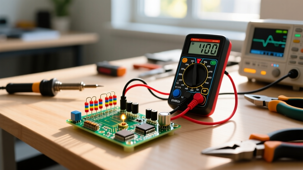
No. A standard digital multimeter (DMM) only measures DC resistance. It applies a small DC current and measures the voltage drop. Because reactance is strictly a function of AC frequency ($X_L = 2\pi fL$ and $X_C = 1 / 2\pi fC$), a DC measurement will show inductors as near-short circuits (just the DC resistance of the wire) and capacitors as open circuits. To measure impedance, you must use an LCR meter, which injects an AC test signal at a specific frequency (e.g., 1kHz or 100kHz), or a Vector Network Analyzer (VNA) for RF/microwave impedance profiling.
When does the inductive reactance of a via ruin my signal integrity?
A standard plated through-hole (PTH) via has roughly 0.5nH to 1.0nH of parasitic inductance. At low frequencies (e.g., I2C at 400kHz or audio signals), the inductive reactance ($X_L$) is a fraction of a milliohm—completely invisible. However, in high-speed digital signals (like DDR4 memory or USB 3.0) where edge rates are in the picoseconds, the frequency content extends well into the gigahertz range. At 5GHz, a 1nH via presents an $X_L$ of 31.4$\Omega$. If your trace is designed for 50$\Omega$, that via creates a massive impedance discontinuity, causing signal reflections, eye-diagram closure, and bit errors. In these cases, you must use back-drilled vias or microvias to eliminate the unused stub inductance.