The transition from a messy breadboard prototype to a manufactured printed circuit board is where most hobbyist and junior engineering projects either succeed or silently fail. A robust PCB design flow isn't just about drawing footprints in KiCad or Altium and clicking auto-route. It requires translating a circuit that relies on the hidden parasitics and high contact resistance of a solderless breadboard into a deterministic, thermally stable copper layout. If you skip the math on trace widths or ignore power rail sag, your first spin will likely end up in the scrap bin.
This guide breaks down the critical physical and electrical checkpoints in the PCB design flow, giving you the exact numbers and bench procedures needed to get a working board on the first fabrication run.
Sizing Traces: The IPC-2221 Current vs. Width Matrix
On a breadboard, a 22 AWG jumper wire can easily carry 2A without noticeable heating. On a PCB, copper thickness (weight) and trace width dictate your thermal limits. If you undersize a trace, the resistance causes a voltage drop and the trace acts as a heater, potentially delaminating the FR4 substrate or lifting pads.
The industry standard for this is IPC-2221 Generic Standard on Printed Board Design. The core metric is temperature rise: how much hotter the trace gets compared to ambient air at a given current. For most commercial and hobbyist designs, a 10°C rise is the standard target. Below is the reference matrix for standard 1oz (35µm) and 2oz (70µm) copper weights.
| Current (A) | 1oz External (mils) | 1oz Internal (mils) | 2oz External (mils) | 2oz Internal (mils) |
|---|---|---|---|---|
| 1.0 A | 10.0 | 20.0 | 6.0 | 12.0 |
| 2.0 A | 30.0 | 60.0 | 18.0 | 35.0 |
| 5.0 A | 110.0 | 225.0 | 65.0 | 130.0 |
| 10.0 A | 280.0 | 575.0 | 165.0 | 330.0 |
The Internal Layer Penalty: Notice that internal layers require roughly double the width of external layers for the same current. This is because external layers benefit from convective air cooling, while internal layers are entombed in FR4 fiberglass, which is a thermal insulator. If your design pushes 5A through an inner power plane on a 4-layer board, you need a massive 225-mil trace on 1oz copper. For high-current paths, always route on external layers or use 2oz copper pours.
For complex impedance and thermal calculations, bypass online calculators and use the industry-standard Saturn PCB Toolkit. It accounts for via thermal relief, trace thickness variations, and specific dielectric materials.
The Breadboard-to-PCB Migration Checklist
Breadboards lie to you. They introduce parasitics that your circuit compensates for, which vanish when you move to a PCB. Here are the specific mistakes that survive the migration and how to fix them in your schematic and layout.
1. Ignoring Parasitic Capacitance and Contact Resistance
Every contact point on a standard solderless breadboard introduces roughly 2pF to 5pF of stray capacitance and 100mΩ to 200mΩ of contact resistance.
- The Mistake: If you tuned a high-impedance op-amp feedback loop or a >1MHz oscillator on a breadboard, the stray capacitance was part of your compensation network. On a PCB, that capacitance disappears, and your circuit will likely oscillate or ring.
- The Fix: Recalculate your compensation networks assuming 0pF stray capacitance. Add optional unpopulated footprint pads for small-value capacitors (e.g., 2pF–10pF) in parallel with feedback resistors so you can tune the board post-fabrication if needed.
2. Power Rail Sag and Ground Bounce
- The Mistake: Breadboard power rails have high resistance. A 500mA load pulling through a breadboard rail will drop 50mV to 100mV before it even reaches the IC. If your analog biasing relied on this "sag," moving to a PCB with a solid, low-impedance copper ground plane will shift your DC operating points.
- The Fix: Never rely on trace resistance for voltage dropping. Use explicit, low-tolerance resistors or LDOs for biasing. Ensure your PCB layout uses a continuous ground plane on Layer 2 to eliminate ground bounce.
3. Decoupling Capacitor Placement
- The Mistake: Placing a 100nF bypass capacitor "near" the IC on a breadboard usually means 2 to 3 inches of jumper wire. That wire adds ~20nH of parasitic inductance, rendering the capacitor useless for high-frequency digital switching noise. If you replicate this distance on a PCB, your microcontroller will brownout under load.
- The Fix: In your PCB layout, place 100nF (X7R ceramic) decoupling capacitors within 2mm to 5mm of the VCC and GND pins. Route the traces directly from the IC pad to the capacitor pad, then to the via—never daisy-chain power through the capacitor pads.
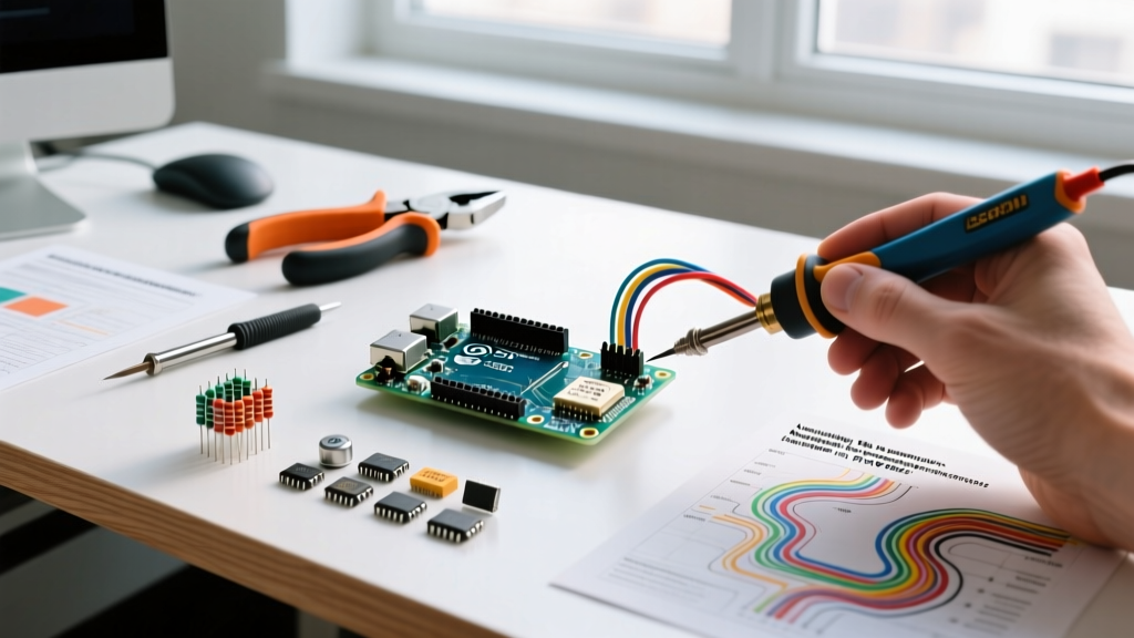
When assembling your first spin, alloy and temperature selection dictate joint reliability. For lead-free assembly, use SAC305 (Sn96.5/Ag3.0/Cu0.5) wire with a rosin-core flux. Set your soldering station (e.g., Hakko FX-888D or Pinecil) to 350°C–360°C. If you are using traditional Sn63/Pb37 eutectic solder, drop the tip temperature to 320°C to prevent burning the flux and oxidizing the tip.
Fume Extraction is Mandatory: Vaporized rosin and activated flux fumes are known respiratory sensitizers that can cause occupational asthma. Never solder in still air. Use a dedicated HEPA and activated carbon fume extractor (like the Hakko FA-400 or a benchtop hood) positioned 6 to 8 inches from the solder joint to capture the plume before it reaches your breathing zone.
Testing Your First Spin Board: A Step-by-Step Verification
When your boards arrive from the fab house (whether it's JLCPCB, PCBWay, or OSH Park), the biggest mistake you can make is plugging them directly into a wall adapter or USB port. A rigorous first-spin verification protocol protects both your board and your bench equipment.
- Visual and DFM Inspection: Before picking up a soldering iron, inspect the bare board under a 10x loupe or microscope. Look for solder mask slivers over pads, drill hits that are off-center, and broken silkscreen. Verify that the board thickness matches your order (e.g., 1.6mm) using digital calipers.
- Dead-Bug Continuity Check: Set your multimeter to continuity (beep) mode. Place the probes on the main VCC and GND test points. You should read an open circuit (OL) or a slow-rising resistance as input capacitors charge. If it reads a dead short (< 2 ohms), stop. You likely have a solder bridge under an IC pad or a fab error causing an internal plane short.
- Current-Limited Power Up: Never use a dumb USB wall brick for first power. Use a programmable bench supply (like a Rigol DP832 or Korad KA3005P). Set the voltage to your exact VCC (e.g., 3.30V) and set the current limit (OCP) to 150% of your calculated quiescent draw. If your board is expected to idle at 50mA, set the limit to 75mA. Turn on the output. If the supply hits current limit and the voltage drops to near zero, you have a fault. Power down and troubleshoot.
- Thermal Sweep: If the board powers up successfully, let it run for 5 minutes. Scan the board with an infrared thermal camera (like a FLIR One) or an infrared thermometer. Look for localized hot spots on ICs, LDOs, or vias. An LDO dropping 12V to 3.3V at 200mA will dissipate 1.74W; if it's in a SOT-223 package without a adequate thermal via array, it will quickly exceed its 125°C junction limit.
- Signal Integrity and Ripple Check: Connect an oscilloscope probe to the main 3.3V or 5V rail. Use AC coupling and set the vertical scale to 20mV/div. Trigger on the rising edge of your system clock or switching regulator frequency. The power rail ripple should be clean and typically less than 50mV peak-to-peak for sensitive digital logic. If you see massive 200mV spikes, your decoupling capacitors are either the wrong value, placed too far away, or you have a ground loop issue in your layout.
By treating the PCB design flow as a series of verifiable physical constraints rather than just a software routing exercise, you eliminate the guesswork. Calculate your trace widths against IPC standards, design out the breadboard parasitics, and test with current-limited precision. Your first spin will power up exactly as intended.