
The Integrator Op Amp: Symbol, Pinout, and Core Operation
An integrator op amp is an analog computing circuit where the output voltage is directly proportional to the time-integral of the input voltage. Unlike standard inverting amplifiers that use a feedback resistor, the integrator replaces that resistor with a capacitor ($C_f$). As input current flows through the input resistor ($R_{in}$), it charges the feedback capacitor, causing the output voltage to ramp linearly over time.
The governing formula for the ideal output voltage is:
$V_{out}(t) = -\frac{1}{R_{in}C_f} \int_{0}^{t} V_{in}(\tau) d\tau + V_{initial}$
Symbol and Pinout Description
In schematic diagrams, the integrator is drawn using the standard operational amplifier triangle symbol. The non-inverting input (+) is typically tied to ground (or a virtual ground reference). The inverting input (-) is the summing junction, connected to the input signal via $R_{in}$ and to the output via $C_f$.
For physical wiring, we typically use a standard 8-pin DIP (Dual In-line Package) footprint. Using the ubiquitous TL072 dual op amp as our reference, the pinout is:
- Pin 1: Output A
- Pin 2: Inverting Input A (-)
- Pin 3: Non-Inverting Input A (+)
- Pin 4: V- (Negative Supply Rail)
- Pin 5: Non-Inverting Input B (+)
- Pin 6: Inverting Input B (-)
- Pin 7: Output B
- Pin 8: V+ (Positive Supply Rail)
Because the non-inverting input (Pin 3) is grounded, the op amp's high open-loop gain forces the inverting input (Pin 2) to remain at 0V. This is known as a virtual ground. All input current therefore flows entirely into the feedback capacitor, enabling precise mathematical integration.
Selecting and Biasing the Right Op Amp (Safe Defaults)
The silent killer of integrator circuits is input bias current ($I_B$). In a real op amp, a tiny amount of DC current flows into or out of the input pins. In an integrator, this bias current has nowhere to go but into the feedback capacitor. Over time, $I_B$ charges $C_f$, causing the output to drift relentlessly toward the supply rail even when the input signal is zero. The drift rate is calculated as $dV/dt = I_B / C_f$.
Therefore, you must select an op amp with FET or CMOS inputs, which offer picoamp-level bias currents, rather than bipolar inputs which operate in the nanoamp or microamp range.
Op Amp Selection Matrix for Integrators
| Part Number | Input Type | Typical $I_B$ | Slew Rate | Supply Range | Best Application |
|---|---|---|---|---|---|
| TL072 | JFET | 5 pA | 13 V/µs | ±5V to ±18V | Safe default for general-purpose analog integration and audio. |
| OPA2134 | FET | 2 pA | 20 V/µs | ±2.5V to ±18V | Precision instrumentation, high-end PID controllers. |
| MCP6002 | CMOS | 1 pA | 0.6 V/µs | 1.8V to 6.0V (Single) | Battery-powered, single-supply microcontroller interfaces. |
| LM358 | Bipolar | 20 nA | 0.3 V/µs | 3V to 32V (Single) | Avoid for precision. Only use for slow, low-cost DC ramp generators. |
Biasing for Dual vs. Single Supply
For true AC signal integration (like converting a square wave to a triangle wave), a dual power supply (e.g., ±12V or ±15V) is mandatory. This allows the output to swing symmetrically above and below 0V. Tie Pin 4 to -15V, Pin 8 to +15V, and Pin 3 to system ground.
If you are forced to use a single supply (e.g., +12V and GND), you must create a virtual ground at $V_{CC}/2$ (e.g., +6V) using a resistor voltage divider buffered by another op amp. Pin 3, as well as the ground reference for your input signal, must tie to this +6V virtual ground so the output has room to swing both up and down.
Complete Application Circuit: Precision Analog Integrator
An "ideal" integrator has infinite DC gain, meaning any microscopic DC offset will eventually saturate the output. A practical integrator adds a high-value feedback resistor ($R_f$) in parallel with $C_f$. This limits the low-frequency gain and turns the circuit into a low-pass filter below a specific cutoff frequency, stabilizing the DC operating point.
Component Values and Specifications
- U1: TL072 (JFET Dual Op Amp)
- $R_{in}$: 10 kΩ (Sets input impedance and integration scale)
- $C_f$: 100 nF (Sets the primary time constant)
- $R_f$: 1 MΩ (Limits DC gain to 100, prevents rail saturation)
- Power: ±15V DC (Decouple with 100nF MLCC capacitors close to Pins 4 and 8)
With these values, the integration time constant ($\tau = R_{in} \times C_f$) is 1 millisecond. If you apply a +1V DC step to the input, the output will ramp downward at a rate of 100 V/second (or 0.1 V/ms) until it hits the limit set by $R_f$ or the supply rail.
Never use X7R, Y5V, or electrolytic capacitors for $C_f$ in a precision integrator. High-K ceramics exhibit severe voltage coefficient (capacitance drops as voltage increases) and piezoelectric effects. Electrolytics have high leakage currents that will ruin your integration slope. Always specify C0G/NP0 ceramics for values under 10nF, or polypropylene film capacitors for values 10nF and above. Check the Analog Devices MT-043 Tutorial for deeper math on dielectric absorption.
Failure Modes and Multimeter Testing Guide
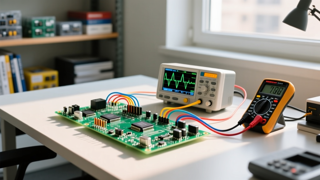
When an integrator circuit fails, it usually manifests as an output pegged to the positive or negative supply rail, or a severely distorted ramp. Here is how to systematically troubleshoot the board using a standard digital multimeter (DMM).
- De-energize and Discharge: Turn off the power. Carefully short the feedback capacitor ($C_f$) with a 1kΩ resistor to discharge any stored voltage. (Shorting it directly with a screwdriver can damage the capacitor's internal metallization over time).
- Verify Passive Components: Switch your DMM to resistance mode. Measure $R_{in}$ and $R_f$. Because they are in-circuit, readings might be slightly lower than nominal due to parallel op-amp impedance. If $R_{in}$ reads open (OL) or drastically high, the resistor is blown. If $R_f$ reads near 0Ω, check for a solder bridge.
- Test the Op Amp Inputs (Diode Mode): Set the DMM to diode test. Place the red probe on Pin 4 (V-) and the black probe on Pin 2 (In-). You should read a forward voltage drop (typically 0.6V for bipolar, or OL for JFET/CMOS inputs like the TL072). Repeat for Pin 3. If you read 0.00V (short) or OL on a bipolar chip, the input stage is blown from Electrical Overstress (EOS).
- Check Supply Voltages: Power the circuit on. Switch the DMM to DC Voltage. Measure Pin 8 to GND (should be +15V) and Pin 4 to GND (should be -15V). If supplies are missing, check your linear regulators or bench supply wiring.
- Verify the Virtual Ground: Measure Pin 3 (Non-inverting input). It must read exactly 0.00V (for dual supply) or $V_{CC}/2$ (for single supply). If this pin is floating or picking up noise, the integrator will amplify that noise and saturate.
- Analyze the Output Ramp: Connect an oscilloscope to Pin 1. If the output is a flat line pegged to -14V, your $C_f$ might be leaky, or the op amp's input offset voltage is too high for the chosen $R_f$ value. Try temporarily shorting $C_f$; if the output snaps back to 0V, the op amp is fine and the issue is DC drift.
Integrator Op Amp FAQ
Why does my integrator op amp output drift to the supply rail?
Output drift is almost always caused by input bias current ($I_B$) or input offset voltage ($V_{os}$) continuously charging the feedback capacitor. If you are using a bipolar op amp like the LM358, the bias current is high enough to saturate the output in seconds. To fix this, either switch to a FET-input op amp (like the TL072 or OPA2134), decrease the value of $R_{in}$ and $C_f$ to speed up the circuit relative to the drift, or add a large feedback resistor ($R_f$) in parallel with $C_f$ to provide a DC bleed path. For more on offset errors, refer to the TI TL072 Datasheet electrical characteristics table.
How do I calculate the feedback capacitor for a specific time constant?
The time constant ($\tau$) of an integrator is simply $\tau = R_{in} \times C_f$. If you need a specific integration slope, rearrange the formula to $C_f = \tau / R_{in}$. For example, if you want a time constant of 5 milliseconds (0.005s) and you have chosen a standard 50 kΩ input resistor, your required capacitance is $0.005 / 50,000 = 100 nF$. Always choose standard E12/E24 capacitor values and adjust $R_{in}$ with a trimmer potentiometer if exact calibration is required.
Can I use an LM358 for a high-frequency integrator op amp circuit?
No. The LM358 has a notoriously low slew rate of about 0.3 V/µs. In an integrator, the output must ramp linearly. If the input frequency is too high, the required output slope will exceed the op amp's slew rate limit. Instead of a clean triangle wave, your output will look like a trapezoid with flattened peaks, introducing massive harmonic distortion. For audio or high-frequency signal processing (above 5 kHz), use an op amp with a slew rate >10 V/µs, such as the TL072 (13 V/µs) or the NE5532 (9 V/µs).
What is the difference between an ideal and practical integrator op amp?
An ideal integrator uses only a capacitor in the feedback loop. Mathematically, it integrates perfectly down to 0 Hz (DC). However, in the real world, an ideal integrator has infinite gain at DC, meaning any microscopic thermal noise or offset voltage will integrate over time and slam the output into the power supply rail. A practical integrator adds a high-value resistor ($R_f$) in parallel with the capacitor. This limits the maximum DC gain to $-R_f / R_{in}$ and creates a low-pass filter corner frequency ($f_c = 1 / (2\pi R_f C_f)$). Below this corner frequency, the circuit acts like a standard inverting amplifier; above it, it acts as a true integrator. You can read more about practical compensation networks on All About Circuits.


