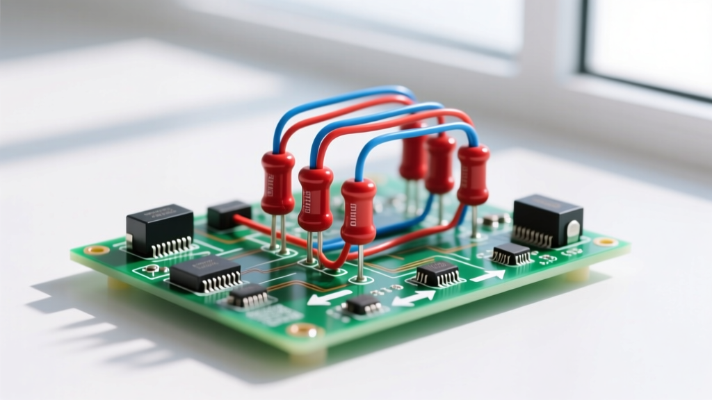

To connect resistors in parallel, you must join all the 'left' leads of the resistors together to form a single shared node (Node A), and join all the 'right' leads together to form a second shared node (Node B). In this configuration, the voltage across Node A and Node B is identical for every resistor, while the total current from the source divides among the parallel branches. The equivalent resistance of the circuit will always be lower than the smallest individual resistor in the parallel bank.
This guide walks through the physical wiring, schematic translation, and bench verification of a parallel resistor network, treating the setup with the same rigor as a formal wiring diagram walkthrough.
Schematic Symbols and Physical Lead Mapping
Before tracing the circuit, we must translate the schematic symbols to the physical component. On a schematic, resistors are represented by either the IEEE standard zigzag line or the IEC standard rectangular box. Regardless of the symbol used, the two ends of the symbol represent the two physical wire leads of the component.
Unlike diodes or electrolytic capacitors, standard through-hole resistors (such as the Vishay PR02 metal film or Yageo CFR carbon film series) are non-polarized. This means there is no functional 'positive' or 'negative' terminal; current can flow in either direction. However, for the sake of diagram tracing and breadboard mapping, we designate the leads based on the physical orientation of the component and the color band reading direction.
| Schematic Designation | Physical Component Lead | Breadboard Node / Row | Circuit Function |
|---|---|---|---|
| Node A (Top) | Lead 1 of R1, Lead 1 of R2 | Row 10 (Tied to V+ Rail) | Common voltage source entry point |
| R1 Branch | Body of R1 | Spans Rows 10 to 15 | Primary current limiting path |
| R2 Branch | Body of R2 | Spans Rows 10 to 15 | Secondary parallel current path |
| Node B (Bottom) | Lead 2 of R1, Lead 2 of R2 | Row 15 (Tied to GND Rail) | Common return / ground path |
Node-by-Node Circuit Trace and Equivalent Resistance Data
With the terminals mapped, we can perform a textual node-by-node trace of the current path from the power source, through the parallel bank, and back to ground. This trace assumes a standard 5V DC bench supply powering two parallel resistors.
- Source Origin: Current leaves the positive terminal of the 5V DC supply and travels via a red jumper wire to Node A (Breadboard Row 10).
- The Split (Node A): At Node A, the conductive path splits. Electrons do not 'choose' a path; rather, current divides proportionally based on the conductance (1/R) of each branch. Current enters Lead 1 of R1 and Lead 1 of R2 simultaneously.
- The Branches: Current flows through the resistive element of R1 and R2. Because the voltage across both is locked at 5V, the branch with the lower resistance will draw a higher share of the total current (per Ohm's Law, I = V/R).
- The Recombination (Node B): The current exits Lead 2 of R1 and Lead 2 of R2, recombining at Node B (Breadboard Row 15). The total current at Node B is exactly equal to the sum of the currents from R1 and R2 (Kirchhoff's Current Law).
- Ground Return: From Node B, the combined current flows through a black jumper wire to the ground (GND) rail, completing the circuit back to the negative terminal of the power supply.
When designing parallel networks, you rarely use random values. You combine standard E24 series values to achieve a specific equivalent resistance ($R_{eq}$) or to increase the total power dissipation capability of the bank. The formula for two parallel resistors is $R_{eq} = (R1 \times R2) / (R1 + R2)$.
| R1 Value | R2 Value | Equivalent Resistance ($R_{eq}$) | Total Current Draw | Current through R1 / R2 |
|---|---|---|---|---|
| 100 Ω | 100 Ω | 50.0 Ω | 100.0 mA | 50.0 mA / 50.0 mA |
| 220 Ω | 330 Ω | 132.0 Ω | 37.8 mA | 22.7 mA / 15.1 mA |
| 1.0 kΩ | 1.0 kΩ | 500.0 Ω | 10.0 mA | 5.0 mA / 5.0 mA |
| 4.7 kΩ | 10.0 kΩ | 3,197 Ω (3.2 kΩ) | 1.56 mA | 1.06 mA / 0.50 mA |
| 10.0 kΩ | 100.0 kΩ | 9,090 Ω (9.1 kΩ) | 0.55 mA | 0.50 mA / 0.05 mA |
As shown in the data above, when a 10 kΩ resistor is placed in parallel with a 100 kΩ resistor, the 10 kΩ resistor dominates the circuit, pulling the equivalent resistance down close to its own value and carrying 90% of the total current. For a deeper mathematical breakdown of parallel DC networks, refer to the parallel resistor chapter on All About Circuits.
Step-by-Step Physical Wiring Procedure
Whether you are prototyping on a solderless breadboard or building a permanent circuit on a perfboard, the physical execution of the parallel connection requires attention to lead preparation and node integrity.
Breadboard Prototyping
- Prepare the Leads: Use flush cutters to trim the resistor leads so they extend about 1/4 inch (6mm) past the resistor body. Bend the leads downward at a 90-degree angle using needle-nose pliers, ensuring the spacing matches the breadboard's 0.1-inch (2.54mm) grid.
- Insert R1: Push Lead 1 of R1 into Row 10, Column A. Push Lead 2 of R1 into Row 15, Column A.
- Insert R2: Push Lead 1 of R2 into Row 10, Column B (sharing the same internal copper clip as R1's Lead 1). Push Lead 2 of R2 into Row 15, Column B.
- Wire the Nodes: Insert a red jumper wire from the positive power rail to Row 10, Column C. Insert a black jumper wire from the ground rail to Row 15, Column C.
Perfboard Soldering
- Mount the Components: Insert both resistors through the perfboard so their leads sit in adjacent holes on the top copper pads (e.g., R1 in holes A1/A5, R2 in holes B1/B5).
- Create Node A: On the solder side, use a piece of bare tinned copper wire to bridge the pads for R1-Lead1 and R2-Lead1. Apply a 350°C iron and 60/40 rosin-core solder to create a single, shiny solder joint connecting both leads and the bridge wire.
- Create Node B: Repeat the bridging and soldering process for R1-Lead2 and R2-Lead2 on the opposite end of the board.
- Trim and Inspect: Clip the excess leads flush with the solder joints. Inspect for 'cold' solder joints (which look dull and grainy) or solder bridges to adjacent, unintended pads.
Multimeter Verification and Troubleshooting
Verifying a parallel resistor network with a digital multimeter (DMM) like the Fluke 87V requires understanding the difference between in-circuit and out-of-circuit measurements. A common beginner mistake is attempting to measure the value of a single resistor while it remains wired in parallel with other components.
How to Verify the Total Equivalent Resistance (In-Circuit)
If you want to verify that your wiring matches the schematic's $R_{eq}$ calculation:
- Set your DMM to the Resistance (Ω) mode. If it is not auto-ranging, select a range higher than your expected $R_{eq}$ (e.g., the 2kΩ or 20kΩ setting).
- Place the red probe on Node A and the black probe on Node B.
- Read the display. For a parallel bank of a 220Ω and 330Ω resistor, the meter should read approximately 132Ω.
- Edge Case: If the meter reads 'OL' (Over Limit) or infinity, you have an open circuit. Check for a broken lead or a cold solder joint at Node A or Node B.
How to Verify Individual Resistors (Out-of-Circuit)
If you need to verify the tolerance and exact value of R1 or R2 individually, you cannot do this while they are wired in parallel. The DMM will simply read the combined equivalent resistance of the entire network. Furthermore, if the parallel bank is connected to an active circuit board, semiconductor junctions and IC traces will create hidden parallel paths, rendering the resistance reading completely invalid. For accurate individual verification, follow the Fluke guidelines on measuring resistance:
- Desolder or lift one lead of the resistor out of the breadboard/perfboard to isolate it from Node A or Node B.
- Hold the DMM probes firmly against the bare metal of the two isolated leads. Avoid touching the metal probe tips with your fingers, as your body's skin resistance (typically 10kΩ to 100kΩ depending on moisture) will introduce a parallel path and skew high-value resistor readings.
- Compare the measured value against the resistor's color code and tolerance rating (e.g., a 100Ω 5% resistor must read between 95Ω and 105Ω).
By mapping the physical leads to schematic nodes, executing a clean physical connection, and verifying the math with a DMM, you ensure your parallel resistor network will perform exactly as designed under load.


