
The Anatomy of the ESP32 Silicon
When makers first transition from the Arduino Uno to the ESP32, the sheer density of the ESP32 pinout can be overwhelming. With up to 48 GPIO pins on the raw silicon (though typically 30 to 38 are exposed on standard ESP32-WROOM-32E dev boards), understanding the physical layout is only half the battle. The true challenge lies in understanding the internal architecture that dictates what each pin can actually do at any given moment.
Unlike simpler 8-bit microcontrollers where a pin is hardwired to a specific peripheral, the ESP32 utilizes a highly flexible internal routing system. Before assigning a pin to your next sensor or relay, you must understand the difference between the IO_MUX and the GPIO Matrix, as these hardware features dictate the performance and limitations of your circuit.
The IO_MUX vs. The GPIO Matrix
The ESP32 routes signals through two primary pathways. The IO_MUX is a direct, low-latency hardware connection between specific pins and core peripherals like UART0, SPI flash, and I2C. If you use the default pins for I2C (GPIO 21 for SDA, GPIO 22 for SCL), the signal bypasses the matrix, resulting in higher maximum frequencies and lower CPU overhead.
Conversely, the GPIO Matrix is a programmable switch matrix that allows almost any peripheral to be mapped to almost any pin. While this offers incredible design flexibility, routing high-speed signals (like SPI or I2C) through the GPIO Matrix introduces propagation delays and limits the maximum reliable clock speed. For high-speed SPI displays, always consult the official Espressif datasheet to find the dedicated IO_MUX pins.
Decoding the Pinout Matrix: Safe vs. Restricted
Not all pins on an ESP32 development board are created equal. Some are hardwired to the onboard SPI flash memory, some are input-only, and others will cause your board to enter a boot loop if pulled to the wrong logic level during startup.
The 'Safe' GPIOs for General I/O
If you are wiring up standard digital outputs, relays, or basic sensors, you want to use 'safe' pins. These pins do not control boot modes, do not conflict with the Wi-Fi radio, and support both input and output operations. The generally accepted safe pins on a standard ESP32-WROOM module are:
- GPIO 4, 5, 16, 17, 18, 19, 21, 22, 23, 32, 33
These pins are your workhorses. Use them for I2C buses, SPI peripherals, PWM outputs for motor drivers, and standard digital reads.
The ADC2 and Wi-Fi Hardware Conflict
One of the most common stumbling blocks for ESP32 beginners is the Analog-to-Digital Converter (ADC). The ESP32 features two ADC units: ADC1 and ADC2. ADC1 (GPIO 32-39) operates independently and can be used simultaneously with Wi-Fi or Bluetooth.
ADC2 (GPIO 0, 2, 4, 12, 13, 14, 15, 25, 26, 27), however, shares internal hardware resources with the Wi-Fi radio. If Wi-Fi is enabled, ADC2 is completely locked out. If you attempt to read an analog sensor on GPIO 26 while running a Wi-Fi web server, your code will fail silently or return garbage data. Always prioritize ADC1 pins for analog sensors in IoT applications.
Boot Modes and Strapping Pins Explained
Strapping pins are sampled by the ESP32 bootloader during a reset or power-on event. The logic levels (HIGH or LOW) on these pins dictate the boot mode, flash voltage, and debug output. If you wire external components to these pins without considering their boot-state requirements, your ESP32 will fail to upload code or fail to boot entirely.
The Four Primary Strapping Pins
- GPIO 0: Determines boot mode. Must be HIGH for normal SPI flash boot. If pulled LOW during reset, the ESP32 enters the serial bootloader (flash mode). Avoid connecting relays or pull-down resistors to this pin.
- GPIO 2: Determines the SPI flash type. Must be LOW or floating to boot from the internal SPI flash. Connecting an LED with a pull-up resistor here will cause boot failures.
- GPIO 12 (MTDI): Selects the flash voltage regulator (3.3V vs 1.8V). On most modern WROOM-32E modules, this is configured via eFuse, but pulling it HIGH on older boards can cause brownouts and boot loops.
- GPIO 15: Controls boot debug log output. If HIGH, the bootloader prints logs to UART0 at 115200 baud. If LOW, boot logs are silenced.
Pro-Tip: If you must use a strapping pin for a peripheral, ensure your external circuit does not force the pin into the 'wrong' state during the first 100 milliseconds of power-on. Using a transistor or a secondary GPIO to control the peripheral's power state after boot is a reliable workaround.
RTC GPIOs and Deep Sleep Wakeup
When designing battery-powered IoT nodes, the ESP32's Deep Sleep mode is essential. However, when the chip enters deep sleep, the main digital power domain is shut off. Only the Real-Time Clock (RTC) domain remains active.
To wake the ESP32 from deep sleep using an external trigger (like a PIR motion sensor or a reed switch), you must use an RTC-capable GPIO. On the original ESP32, these are GPIO 0, 2, 4, 12-15, 25-27, and 32-39. If you wire your wake-up button to a non-RTC pin like GPIO 16, the chip will never receive the wake-up interrupt and will remain asleep until a hard manual reset.
Power Distribution and Current Limits
A frequent misconception is that the ESP32 development board can act as a robust 5V or 3.3V power supply for an entire project. While the VIN or 5V pin is tied directly to the USB 5V line (limited by your USB port or cable, typically 500mA to 1A), the 3V3 pin is fed through an onboard linear regulator (LDO).
Most cheap dev boards use an AMS1117-3.3 LDO. This regulator must drop 5V down to 3.3V, dissipating the difference as heat. Furthermore, the ESP32 silicon itself can draw current spikes of up to 500mA during Wi-Fi transmission bursts. If you attempt to power external sensors, displays, or relays drawing more than 100mA-200mA from the board's 3V3 pin, the LDO will overheat, trigger thermal shutdown, or cause the ESP32 to brownout and reset. Always use an external buck converter for high-current 3.3V peripherals.
Practical Pin Selection Framework
Use the following decision matrix to assign pins efficiently and avoid hardware conflicts. For deeper API implementation details, refer to the ESP-IDF GPIO API documentation.
| Application Need | Recommended Pins | Pins to Avoid | Technical Reasoning |
|---|---|---|---|
| Analog Sensors (IoT) | GPIO 32, 33, 34, 35, 36, 39 | GPIO 0, 2, 4, 12-15, 25-27 | ADC1 is Wi-Fi independent; ADC2 is blocked during Wi-Fi TX/RX. |
| High-Speed SPI (Displays) | GPIO 14 (SCK), 15 (MOSI), 27 (MISO) | Any pin via GPIO Matrix | Uses dedicated IO_MUX for maximum clock speed and signal integrity. |
| I2C Sensors | GPIO 21 (SDA), 22 (SCL) | GPIO 16, 17 | Default IO_MUX pins. Avoid pins lacking internal pull-ups if possible. |
| Deep Sleep Wake-Up | GPIO 4, 25, 26, 27, 32, 33 | GPIO 16, 17, 18, 19, 21, 22, 23 | Only RTC-domain pins remain powered to detect state changes in sleep. |
| Relays & Motors | GPIO 5, 16, 17, 18, 23 | GPIO 0, 2, 12 | Prevents accidental triggering during the boot-up sequence. |
Common Pitfalls When Reading Diagrams
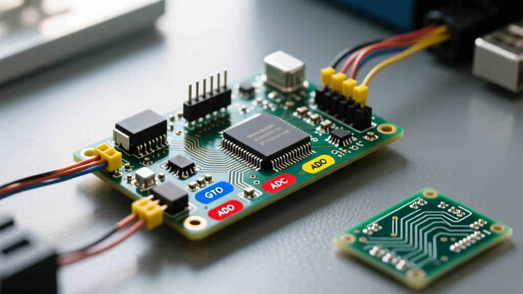
Finally, be wary of silkscreen labeling discrepancies. Unlike the ESP8266 NodeMCU boards which often labeled pins as 'D0' through 'D8' (mapping to completely different internal GPIO numbers), most ESP32 dev boards label pins directly by their GPIO number (e.g., 'GPIO 13' or just '13'). However, some third-party clones still use 'D' prefixes or analog 'A' prefixes that do not match the silicon. Always verify the physical pinout against the specific schematic of your exact development board manufacturer, and rely on the GPIO number in your Arduino IDE or ESP-IDF code.
Furthermore, remember that GPIO 34, 35, 36, and 39 are input-only. They lack internal pull-up and pull-down resistors and cannot drive an LED or output a digital HIGH signal. Attempting to use pinMode(34, OUTPUT) will compile successfully but will result in zero physical voltage change on the pin, leading to hours of frustrating debugging.