
The Hidden Cost of Counterfeit Transistors in Inventory
When sourcing electronic components from gray-market distributors, AliExpress vendors, or unauthorized brokers, the risk of receiving counterfeit, re-marked, or salvaged transistors is alarmingly high. According to data tracked by ERAI's counterfeit parts database, transistors and MOSFETs consistently rank among the most frequently counterfeited semiconductors in the global supply chain. A batch of fake IRFZ44N MOSFETs or re-marked 2N2222 BJTs slipping into your production inventory doesn't just cause prototype failures; it leads to catastrophic field returns and damaged brand reputation.
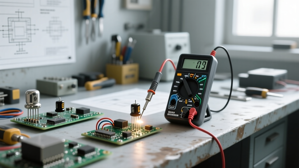
For hardware engineers, lab managers, and procurement specialists, establishing a rigorous incoming quality control (QC) protocol is non-negotiable. While dedicated curve tracers and automated optical inspection (AOI) machines are ideal for high-volume manufacturing, the backbone of any DIY lab or small-batch prototyping facility is the digital multimeter (DMM). Mastering the testing of transistor using multimeter techniques allows you to rapidly verify junction integrity, identify gross failures, and spot suspicious anomalies before components are logged into your inventory management system.
Setting Up a High-Throughput Transistor Testing Station
Batch testing hundreds of TO-92 or TO-220 packaged transistors requires a multimeter that balances speed, accuracy, and ergonomic probe handling. Not all DMMs are created equal when it comes to semiconductor diagnostics.
Essential Multimeter Features for Batch QC
- Fast Continuity and Diode Test Response: When sweeping through a tape-and-reel batch of 2N3904 BJTs, a slow auto-ranging multimeter will destroy your throughput. The Fluke 87V remains the gold standard here, offering near-instantaneous diode test readings and an audible continuity beep that triggers at less than 100 ohms.
- Open Lead Voltage (Diode Mode): Standard silicon PN junctions require about 0.6V to 0.7V to forward-bias. However, testing certain MOSFET gates or Schottky-integrated packages may require a DMM that outputs at least 2.5V to 3.0V in diode test mode. Budget meters like the AN8008 often output less than 1.5V, which can result in false 'Open' (OL) readings on specific compound semiconductor junctions.
- hFE Testing Sockets: While basic junction testing identifies dead shorts, it doesn't verify gain. Multimeters like the Uni-Trend UT61E+ feature dedicated hFE (Beta) sockets, allowing you to sort inventory into matched bins—a critical step for audio amplifier differential pairs.
Pro-Tip for Inventory Stations: Mount your multimeter on an articulating arm and use heavy-duty, spring-loaded test probes (like Pomona electronics probes) to reduce hand fatigue during extended QC sessions.
Step-by-Step: Testing of Transistor Using Multimeter
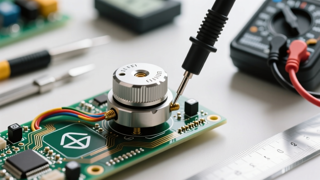
The core methodology for verifying discrete semiconductors relies on the DMM's diode test function. This mode sources a small, constant current (usually 1mA to 2mA) and measures the resulting voltage drop across the junction. Below is the definitive framework for testing the two most common transistor families in your inventory.
BJT (Bipolar Junction Transistor) Diode Test Method
A BJT is essentially two back-to-back diodes sharing a common terminal (the Base). Whether you are testing an NPN (e.g., 2N3904) or PNP (e.g., 2N3906), the procedure remains structurally similar, with probe polarity reversed. As detailed in Fluke's official transistor testing guide, you must verify three distinct states:
- Base-Emitter (B-E) Junction: Place the Red probe on the Base and Black on the Emitter (for NPN). Expect a reading between 0.600V and 0.750V.
- Base-Collector (B-C) Junction: Place the Red probe on the Base and Black on the Collector. Expect a similar reading, usually slightly lower (e.g., 0.580V to 0.700V) due to the physical doping differences in the collector region.
- Collector-Emitter (C-E) Path: Place probes across Collector and Emitter in both polarities. Both must read OL (Over Limit / Open). Any reading below OL indicates a shorted die or severe thermal damage.
MOSFET Gate Charge and Body Diode Verification
Testing a MOSFET (like the ubiquitous IRF3205 or IRFZ44N) is fundamentally different from a BJT because the Gate is electrically insulated by a layer of silicon dioxide. Relying solely on a diode test is insufficient; you must also test the gate's capacitive charge retention. SparkFun's transistor tutorial provides excellent foundational theory, but for inventory QC, use this advanced field technique:
- Discharge the Gate: Short the Gate (G) and Source (S) pins together with your probe or a piece of wire to drain any residual parasitic capacitance.
- Verify the Body Diode: Set the DMM to Diode mode. For an N-Channel MOSFET, place the Red probe on the Source and Black on the Drain. You should read the body diode forward voltage drop (typically 0.400V to 0.600V). Reversing the probes should yield OL.
- The Gate Charge Test: While keeping the Black probe on the Source, briefly touch the Red probe to the Gate. The multimeter's internal voltage will charge the gate capacitance, turning the MOSFET 'ON'.
- Verify Conduction: Move the Red probe back to the Drain (Black remains on Source). The multimeter should now read near 0.000V (or trigger the continuity beep), proving the channel is fully enhanced. Short G to S again, and the reading should immediately return to the body diode drop or OL, confirming the gate insulation is intact and not suffering from punch-through leakage.
Expected Multimeter Readings Reference Table
Keep this reference chart at your QC station to quickly cross-reference incoming batches against known-good specifications.
| Component Type | DMM Mode | Probe Placement (Red / Black) | Expected Reading (Pass) | Failure Mode Indicated |
|---|---|---|---|---|
| NPN BJT (e.g., 2N2222) | Diode | Base / Emitter | 0.620V - 0.680V | OL (Open die) or 0.00V (Short) |
| PNP BJT (e.g., BC557) | Diode | Emitter / Base | 0.600V - 0.700V | OL (Open die) or 0.00V (Short) |
| N-Ch MOSFET (e.g., IRFZ44N) | Diode | Source / Drain | 0.450V - 0.550V | 0.00V (Shorted channel/die) |
| N-Ch MOSFET (Gate Test) | Diode | Drain / Source (Post-Charge) | 0.000V - 0.050V | OL (Gate oxide punctured/dead) |
Decoding hFE: Why Beta Matters for Matched Pairs
While the diode test confirms a transistor isn't dead, it tells you nothing about its amplification factor (hFE or Beta). In standard digital logic or switching applications, a wide hFE variance is acceptable. However, if your inventory is destined for precision analog circuits, push-pull audio outputs, or differential amplifier stages, mismatched hFE will cause severe thermal runaway or DC offset errors.
When using a multimeter's hFE socket, be aware of its limitations. Most DMMs inject a very low base current (around 10µA). This is perfectly adequate for small-signal transistors like the BC547. However, testing power transistors like the TIP31C or 2N3055 in a standard DMM socket will yield artificially low and inconsistent hFE readings because the base current is insufficient to properly bias the large silicon die. For power transistor inventory binning, invest in a dedicated component tester based on the ATmega328 architecture (like the TC1 or Mega328), which can source higher currents and measure junction capacitance simultaneously.
Red Flags: Identifying Re-marked and Salvaged Components
Multimeter testing will catch electrical failures, but it won't catch a re-marked chip that happens to share the same pinout and basic junction characteristics. For instance, unscrupulous vendors frequently sand down cheap 2N3904 dies and laser-print them as more expensive, higher-current 2N2222 transistors. Both will pass a basic multimeter diode test, but the 2N3904 will melt under a 600mA load.
To protect your inventory, pair your multimeter testing with visual inspection:
- The Acetone Test: Rub the top of the TO-92 or TO-220 package with a Q-tip soaked in acetone. Genuine laser markings will not smear. If black paint rubs off, the part has been 'blacktopped' to hide original markings.
- Lead Inspection: Salvaged transistors pulled from e-waste often have bent leads, uneven lengths, or a dull, oxidized matte finish on the tinning. Fresh inventory from authorized distributors (like Mouser or Digi-Key) will have bright, uniform, and perfectly straight leads.
- Package Weight and Thickness: Counterfeit power MOSFETs often use undersized lead frames to save on copper costs. If an IRF3205 feels suspiciously light or the metal tab is noticeably thinner than a known-good reference sample, reject the batch.
Inventory Management: Binning and Labeling Tested Batches
Once a batch passes the multimeter QC protocol, proper inventory handling is required to maintain traceability. Never mix tested and untested components. Use static-shielding ESD bags for all MOSFETs and sensitive JFETs, as the gate oxide can be destroyed by electrostatic discharge long before the part ever reaches a soldering iron.
Implement a color-coded binning system using adhesive dots on your ESD bags or component drawers. For example, use Green dots for hFE 100-200, Blue for 200-300, and Yellow for 300+. Always log the distributor name, date code, and QC technician's initials into your inventory database. By rigorously applying these testing of transistor using multimeter methodologies, you transform your component storage from a liability into a reliable, production-ready asset.