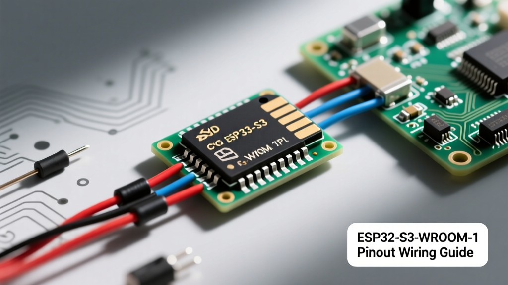

The Anatomy of the ESP32-S3-WROOM-1 Module
The ESP32-S3-WROOM-1 represents a massive leap forward in Espressif’s microcontroller lineup. Featuring a dual-core Xtensa LX7 processor running at 240 MHz, native USB OTG, and vector instructions for AI acceleration, it is a powerhouse for modern IoT and edge-computing projects. However, transitioning from the original ESP32 or the ESP8266 to this chip requires a fundamental shift in how you approach hardware design. Understanding the ESP32-S3-WROOM-1 pinout is the critical first step to avoiding silent failures, bootloops, and peripheral conflicts.
Unlike older microcontrollers where pins were strictly hardcoded to specific functions, the S3 utilizes a highly flexible GPIO Matrix. This allows you to route almost any internal peripheral signal (like UART, I2C, or SPI) to nearly any physical pin. While this offers incredible breadboard flexibility, it also introduces hidden traps regarding signal integrity, internal memory routing, and boot strapping. In this comprehensive tutorial, we will decode the pinout, identify safe GPIOs for your sensors and actuators, and explore advanced hardware configurations.
Decoding the ESP32-S3-WROOM-1 Pinout: Safe vs. Unsafe GPIOs
The ESP32-S3-WROOM-1 module exposes up to 45 programmable GPIOs. However, not all GPIOs are created equal. Some are hardwired to internal flash memory, some dictate the boot sequence, and others are shared with the RF subsystem. Below is a master reference table to help you select the right pins for your next PCB or breadboard layout.
| GPIO Range | Primary Function | Safe for General I/O? | Maker Notes & Warnings |
|---|---|---|---|
| GPIO0, 3, 45, 46 | Strapping Pins | No (Use with Caution) | Dictate boot mode and VDD_SPI voltage. Pulling these low/high incorrectly causes bootloops. |
| GPIO19, 20 | Native USB (D-, D+) | Yes (If USB unused) | Required for native USB Serial/JTAG. Avoid if using the onboard USB-C port. |
| GPIO26 - GPIO32 | Internal SPI Flash | No | Connected internally to the SPI flash chip. Not broken out or usable on WROOM-1. |
| GPIO33 - GPIO37 | Octal SPI (PSRAM/Flash) | Conditional | Consumed internally ONLY on modules with Octal SPI (e.g., N8R8). Safe on Quad SPI modules. |
| GPIO1 - GPIO18 | General Purpose / ADC1 | Yes | Excellent for sensors, I2C, and PWM. ADC1 is safe to use alongside Wi-Fi. |
| GPIO38 - GPIO48 | General Purpose / ADC2 | Yes (With caveats) | ADC2 channels may conflict with Wi-Fi/BT active scanning. Prefer ADC1 for analog sensors. |
The Strapping Pin Trap (And How to Avoid Bootloops)
The most common point of failure for beginners wiring the ESP32-S3-WROOM-1 is ignoring the strapping pins. During the reset sequence, the chip samples the voltage levels on GPIO0, GPIO3, GPIO45, and GPIO46 to determine its boot behavior. If you wire a relay, a low-side switch, or an external pull-down resistor to these pins, the module may enter an unintended download mode or fail to boot entirely.
- GPIO0: Must be HIGH for standard SPI flash boot. If pulled LOW, the chip enters ROM download mode.
- GPIO3: Determines the JTAG signal source. HIGH routes JTAG to the USB Serial/JTAG controller; LOW routes it to GPIO pins.
- GPIO45: Selects the VDD_SPI voltage. LOW sets it to 3.3V (standard for most maker modules); HIGH sets it to 1.8V. Warning: Accidentally pulling this HIGH on a 3.3V module can cause brownouts or flash memory corruption.
- GPIO46: Selects the boot log output. Usually left alone, but pulling it low disables ROM boot messages.
Pro-Tip: If you absolutely must use a strapping pin for an output (like an LED on GPIO0), ensure you include a 10kΩ pull-up resistor to 3.3V so the pin defaults to HIGH during the critical 50ms boot sampling window.
Step-by-Step: Wiring Standard Peripherals to the S3
Configuring Native USB (GPIO19 & GPIO20)
One of the most exciting features detailed in the ESP32-S3 Technical Reference Manual is the inclusion of native USB OTG. Unlike the original ESP32, which required an external UART-to-USB bridge (like the CP2102 or CH340), the S3 can handle USB communications directly via GPIO19 (D-) and GPIO20 (D+).
If you are designing a custom PCB and want to eliminate the UART bridge chip to save space and BOM costs, wire a USB-C receptacle directly to GPIO19 and GPIO20. Ensure you include 5.1kΩ pull-down resistors on the CC1 and CC2 lines of the USB-C connector so the host PC recognizes the device. In the Arduino IDE or ESP-IDF, you can then configure the USB CDC (Communications Device Class) to act as a standard Serial port, or use the TinyUSB library to turn the S3 into a native HID keyboard or MIDI controller.
High-Speed SPI and the GPIO Matrix Delay
Because the ESP32-S3 uses a GPIO Matrix to route internal signals to external pins, you have the freedom to assign I2C SDA/SCL or SPI MOSI/MISO to almost any safe GPIO. For slow protocols like I2C (typically 400kHz), this matrix routing is perfectly fine. However, if you are driving a high-resolution TFT display (like an ST7789 or ILI9341) over SPI at 40MHz or 80MHz, the GPIO Matrix introduces slight capacitive delays and signal skew.
According to the ESP-IDF GPIO API Reference, high-speed signals should bypass the matrix and use the dedicated IOMUX pins. For SPI2, try to use the native pins (GPIO11 for MOSI, GPIO12 for SCK, GPIO13 for MISO, and GPIO10 for CS) to ensure rock-solid signal integrity and prevent screen tearing or SPI checksum errors.
Advanced E-E-A-T: Flash vs. PSRAM Octal SPI Pin Conflicts
Here is a hardware nuance that catches even veteran makers off guard. When purchasing an ESP32-S3-WROOM-1 module, you will see part numbers like ESP32-S3-WROOM-1-N8 or ESP32-S3-WROOM-1-N8R8. The "R8" denotes 8MB of PSRAM. What many datasheets gloss over is how that memory is addressed.
Modules with high-density PSRAM (like the N8R8) utilize Octal SPI to achieve the bandwidth necessary for AI audio buffering and camera feeds. Octal SPI requires 8 data lines instead of the standard 4. Where do these extra 4 lines come from? They are stolen directly from the GPIO pool. Specifically, GPIO33, GPIO34, GPIO35, GPIO36, and GPIO37 are internally routed to the PSRAM/Flash chip.
If you design a schematic assuming GPIO35 is available for a limit switch or an ADC reading, and you order an N8R8 module, that pin will be dead on arrival. It is permanently consumed by the internal memory bus. Always verify whether your specific WROOM-1 variant uses Quad or Octal SPI before finalizing your pin assignments. If you need those specific GPIOs, you must downgrade to a Quad-SPI module (like the N8) or switch to the WROOM-2 variant which routes the antenna differently but may offer different pin breakouts.
Final Breadboard Checklist Before Powering Up
Before you connect your 5V USB cable or LiPo battery to your ESP32-S3-WROOM-1 circuit, run through this hardware validation checklist to prevent catastrophic damage or silent firmware failures:
- Power Delivery: The WROOM-1 module itself does not have a 5V-to-3.3V voltage regulator onboard (only the development boards do). If wiring a bare module, supply a clean, regulated 3.3V directly to the 3V3 pin. Ensure your power source can supply at least 500mA to handle Wi-Fi transmission spikes.
- The EN (Enable) Pin: The EN pin must be pulled HIGH (via a 10kΩ resistor to 3.3V) for the chip to run. If left floating, the S3 will randomly reset due to ambient EMI. Add a 100nF capacitor to ground on the EN pin to debounce physical reset buttons.
- ADC Voltage Limits: The ESP32-S3 ADC is designed for a 0V to ~2.5V range (with attenuation). Do not feed a raw 5V analog signal into any ADC pin, or you will permanently damage the internal ADC multiplexer. Use a voltage divider.
- Wi-Fi Antenna Clearance: The WROOM-1 features a built-in PCB antenna. Ensure there are no ground planes, copper pours, or metal enclosure walls directly beneath or immediately in front of the antenna keep-out zone, or your Wi-Fi range will drop from 50 meters to 2 meters.
By respecting the internal architecture of the ESP32-S3-WROOM-1 and treating the pinout as a dynamic system rather than a static map, you unlock the full potential of this incredible microcontroller. Whether you are building a low-power deep-sleep sensor node or a high-speed AI camera rig, proper GPIO management is the foundation of a reliable maker project.