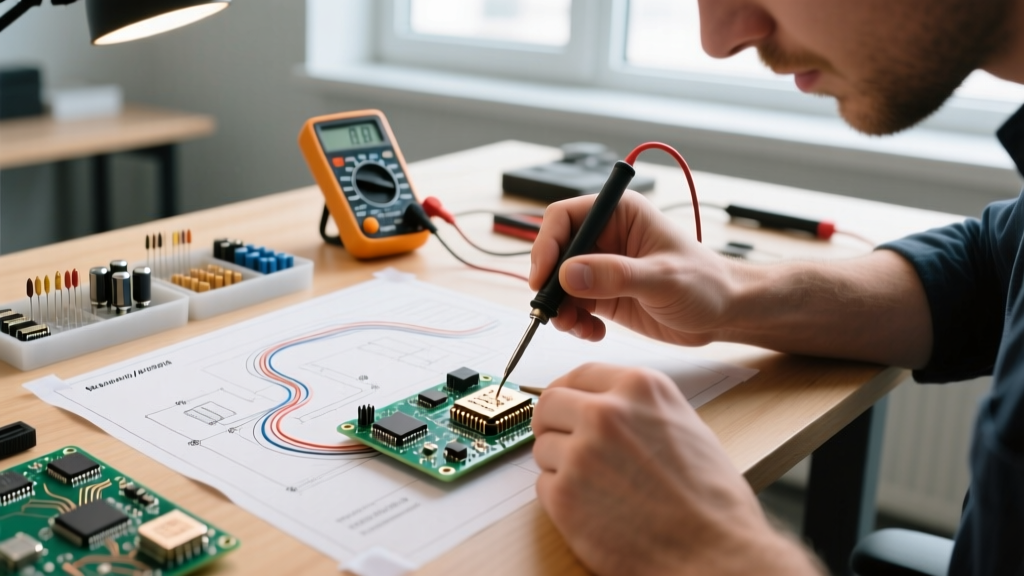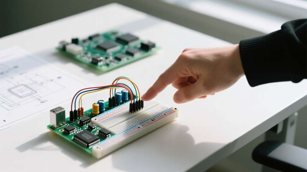

Transitioning from a tangled mess of jumper wires on a solderless breadboard to a clean, professional schematic is a rite of passage for every electronics hobbyist and engineer. While a breadboard is perfect for rapid prototyping, it is a terrible source of truth for final manufacturing. If you are looking to master the breadboard to circuit diagram workflow, you must abandon the temptation to 'draw what you see' and instead learn to abstract physical connections into logical nodes.
The Gap Between Physical Prototypes and Logical Schematics
A common failure mode among beginners is attempting to draw a schematic that visually mimics the physical layout of the breadboard. This results in 'ratsnest' schematics—tangled, unreadable diagrams that are useless for PCB layout or troubleshooting. A schematic represents the logical flow of current and signals, not the geographical placement of components. When executing a breadboard to circuit diagram conversion, your primary goal is to identify electrical nodes. A node is any continuous conductive path. On a standard 830-point breadboard, the inner tie-points are grouped in rows of five, while the outer power rails run continuously (or split in the middle, depending on the manufacturer).
Step 1: Audit and Map the Physical Breadboard
Before opening any CAD software, you must audit your physical prototype. Relying on memory or visual tracing of 24 AWG solid-core wires is a recipe for missed connections and floating pins.
The Continuity Test and Power Rail Trap
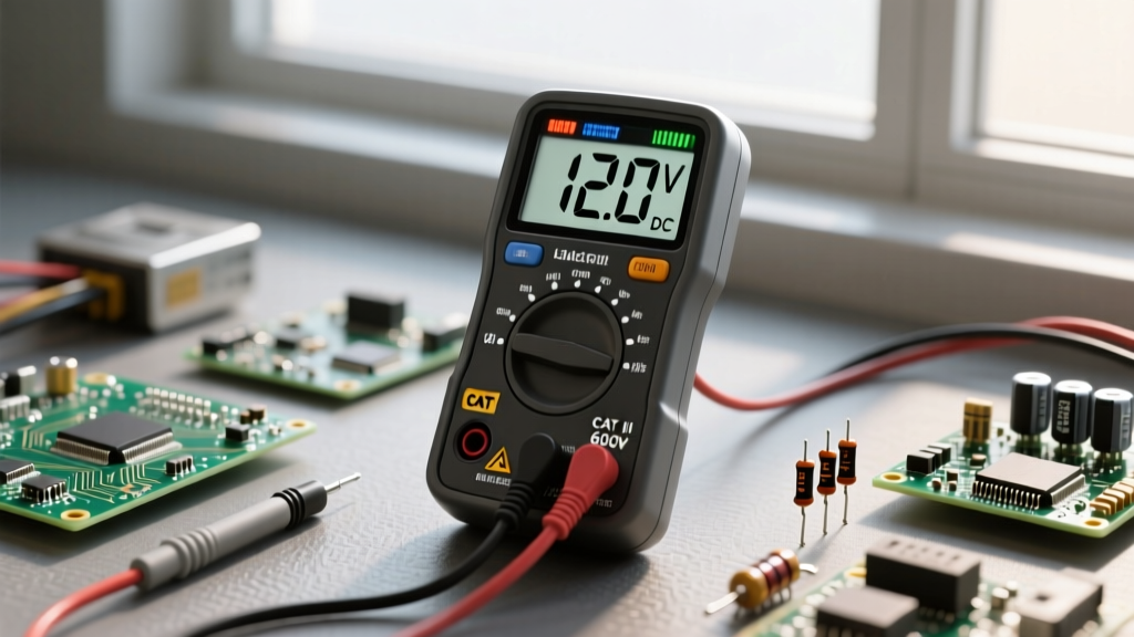
Use a Digital Multimeter (DMM) in continuity mode (the setting with the diode/sound icon) to map every connection. One of the most notorious pitfalls in breadboard prototyping is the 'split power rail.' Many 830-point breadboards have a physical gap in the red and blue lines at the center of the board. If you assume continuity across this gap without testing, your schematic will be fundamentally flawed, leading to unpowered ICs and erratic microcontroller behavior when you move to a PCB.
Pro Tip: Take high-resolution, top-down macro photographs of your breadboard with even lighting. Use a fine-tip marker to label complex ICs and wire harnesses directly on masking tape applied to the components. This physical audit is your baseline reference.
Step 2: Abstracting Nodes for the Schematic Capture
Once the physical connections are verified, you must translate them into a netlist concept. A netlist is a list of all the electrical connections (nets) in your circuit. For example, if Pin 7 of an ATmega328P is connected to a 10kΩ pull-up resistor, and the other end of that resistor connects to the 5V rail, all three of those connection points belong to the same logical node.
Handling Decoupling Capacitors and Ground Bounce
On a breadboard, you are taught to place 100nF (0.1µF) ceramic decoupling capacitors as physically close to the VCC and GND pins of an IC as possible to suppress high-frequency noise. However, in a schematic, these capacitors do not need to be drawn physically 'next' to the IC symbol. Instead, they are logically connected to the VCC and GND nets of that specific IC. Properly representing this in your breadboard to circuit diagram transition ensures that when you eventually route a PCB, the software knows to prioritize short, low-inductance paths for these critical components. For a deeper dive into schematic standards, refer to the SparkFun guide on reading and drawing schematics.
Step 3: Choosing the Right EDA Software
Selecting the right Electronic Design Automation (EDA) tool is critical. While some tools focus on visual breadboard representation, professional workflows require robust schematic capture and PCB layout integration.
| Software | Best For | Learning Curve | Library Management |
|---|---|---|---|
| KiCad 8 | Professional PCB design, complex multi-sheet schematics | Moderate to High | Excellent (built-in + 3rd party) |
| EasyEDA | Quick turnarounds, direct LCSC component integration | Low | Cloud-based, massive user library |
| Fritzing | Visual documentation, basic Arduino tutorials | Very Low | Poor (frequent missing footprints) |
Step 4: Drafting the Schematic with Signal Flow in Mind
When you begin placing symbols in your EDA software, enforce a strict left-to-right signal flow. Inputs (sensors, switches, communication lines) should enter from the left. Processing elements (microcontrollers, op-amps, logic gates) sit in the center. Outputs (LEDs, motors, displays, antennas) exit to the right. Power distribution (voltage regulators, power connectors) is typically placed at the top or bottom of the sheet.
This methodology drastically reduces the cognitive load when reviewing the diagram later. If you are using KiCad, the industry-standard open-source EDA suite, you can leverage hierarchical sheets to break down complex microcontroller circuits into manageable logical blocks (e.g., Power Supply, MCU Core, Motor Drivers). The official KiCad Eeschema documentation provides extensive details on managing hierarchical pins and global labels to keep your breadboard to circuit diagram conversion organized.
Critical Translation Mistakes to Avoid
When moving from a breadboard to circuit diagram, physical proximity often masks logical errors. Here are three specific failure modes that plague DIY electronics projects during the translation phase:
1. The Transistor Pinout Illusion
Breadboard layouts often force you to bend the leads of TO-92 transistors (like the ubiquitous 2N2222 or BC547) to fit the 0.1-inch grid. The physical pinout (Emitter, Base, Collector) might be arranged left-to-right on your breadboard, but the schematic symbol has a specific geometric representation. If you map the breadboard's physical left pin to the schematic's Collector simply because of how it was bent, your PCB footprint will be inverted. Always map logical pins (B, C, E) to schematic pins, regardless of physical wire routing.
2. Missing Flyback Diodes on Inductive Loads
On a breadboard, the long jumper wires and inherent resistance of the cheap spring clips can sometimes accidentally dampen inductive voltage spikes when switching relays or solenoids. This gives a false sense of security. When translating to a schematic, you must explicitly add flyback diodes (like the 1N4148 or 1N4007) across any inductive load. The breadboard hid the problem; the schematic must solve it.
3. Active-Low vs. Active-High Logic Confusion
Microcontroller pins configured as internal pull-ups require switches that connect to ground (active-low). On a breadboard, it is easy to wire a button to VCC by mistake and rely on floating pin states or external resistors to make it 'work.' In the schematic, explicitly use the standard logic bubble (a small circle) on the input pin to denote active-low hardware, ensuring your firmware logic matches the schematic reality. For more on component-level behaviors and physical prototyping realities, consult the Arduino schematic drawing documentation to verify your physical assumptions.
Step 5: Electrical Rules Check (ERC) and Validation
The final and most crucial step is running an Electrical Rules Check (ERC). The ERC algorithm scans your schematic for logical impossibilities and common errors, such as:
- Unconnected Pins: Pins on an IC that have no logical net attached (often a missed ground or enable pin).
- Power Flag Conflicts: Multiple voltage sources driving the same net without a diode or resistor to prevent short circuits.
- Single-Pin Nets: A wire connected to only one component, indicating a broken trace or forgotten connection.
By systematically resolving every ERC warning, you guarantee that the logical diagram perfectly matches the intended electrical behavior of your physical breadboard prototype. Only after a clean ERC should you proceed to footprint assignment and PCB layout, ensuring your transition from prototype to product is flawless.