
Decoding the Pin Diagram of Raspberry Pi for Hardware-Level Optimization
When most makers search for the pin diagram of Raspberry Pi, they are looking for a simple map to blink an LED or wire a basic relay. However, for advanced robotics, high-frequency data acquisition, and low-latency IoT edge nodes, the 40-pin header is a complex landscape of power delivery networks, DMA-capable I/O, and potential electromagnetic interference (EMI) traps. Performance tuning on single-board computers (SBCs) is not just about software overclocking; it requires a deep understanding of physical layer constraints. In this guide, we analyze the Raspberry Pi 4 and 5 GPIO headers through the lens of signal integrity, power rail bottlenecks, and hardware offloading.
Power Rail Bottlenecks: Analyzing Pins 1, 2, 4, and 17
A critical failure mode in high-performance Pi deployments is voltage sag on the 3.3V rail. According to the official Raspberry Pi GPIO documentation, Pins 1 and 17 provide 3.3V power, while Pins 2 and 4 provide 5V. On the Raspberry Pi 4 Model B, the 3.3V rail is generated by an onboard LDO regulator with a strict thermal and current limit. Pulling more than 50mA continuously from the 3.3V pins can cause thermal throttling of the regulator, leading to brownouts and silent data corruption on SPI and I2C buses.
Bypass Capacitor Placement for High-Speed ADCs
If you are interfacing a 1MSPS ADC (like the ADS8861) to the Pi, the transient current spikes during sampling will collapse a weak 3.3V rail. To tune this, you must place a 100nF MLCC ceramic capacitor and a 10uF tantalum capacitor directly across the 3.3V (Pin 1) and Ground (Pin 6) at the point of load. On the Raspberry Pi 5, the RP1 I/O controller manages power distribution differently, offering higher current headroom, but local decoupling remains mandatory for maintaining a signal-to-noise ratio (SNR) above 70dB.
Signal Integrity and Grounding Topologies
The pin diagram of Raspberry Pi features eight dedicated ground pins: 6, 9, 14, 20, 25, 30, 34, and 39. In high-speed digital design, return currents flow in the ground plane directly beneath the signal trace. When using ribbon cables or jumper wires to connect peripherals like high-resolution encoders or LVDS interfaces, inductive loop area becomes your enemy.
Rule of Thumb: For every high-frequency signal line (SPI CLK, I2C SDA) leaving the Pi header, an adjacent ground wire must accompany it to minimize crosstalk and EMI radiation.
For example, if you are routing SPI0 Clock (Pin 23) and MOSI (Pin 19), you should use Pin 20 and Pin 25 as your interleaved grounds in your ribbon cable. Failing to do so will result in severe ringing on the clock edge, causing the peripheral to misread bits at baud rates exceeding 15MHz.
Maximizing Throughput: Hardware SPI vs. Bit-Banging
Software bit-banging GPIO pins to emulate SPI or I2C is a common anti-pattern that destroys CPU performance and introduces microsecond-level jitter. To tune your system for maximum throughput, you must map your peripherals to the dedicated hardware blocks mapped to specific pins.
SPI0 vs. Auxiliary SPI
SPI0 is the primary high-performance bus. Its Chip Select (CE0, CE1), MISO, MOSI, and SCLK are mapped to Pins 24, 26, 21, 19, and 23 respectively. The BCM2835 ARM Peripherals Datasheet details how SPI0 is tied to the DMA controller, allowing zero-CPU-overhead transfers at speeds up to 125MHz (theoretically, though 32MHz is the practical limit for most external ICs due to header capacitance). Conversely, the Auxiliary SPI (SPI1) lacks full DMA support and has a smaller FIFO buffer. Always default to SPI0 pins for high-bandwidth sensors like LiDAR arrays or TFT displays.
Eliminating Jitter: Hardware PWM Pin Selection
Pulse Width Modulation (PWM) is essential for motor control and LED dimming. However, Linux is not a real-time operating system (RTOS). If you use software PWM via libraries like RPi.GPIO, background OS tasks will cause visible flickering and motor cogging. Hardware PWM is driven by dedicated silicon clocks, completely immune to OS scheduling jitter.
On the standard 40-pin header, Hardware PWM0 is available on GPIO 12 (Pin 32) and GPIO 18 (Pin 12). Hardware PWM1 is on GPIO 13 (Pin 33) and GPIO 19 (Pin 35). When tuning a PID control loop for a brushless DC motor, you must wire your ESC or motor driver to these specific pins and configure the dtoverlay=pwm-2chan in your config.txt to achieve a rock-solid 20kHz switching frequency.
Reference Table: Performance-Critical GPIO Assignments
| Function | Physical Pin | GPIO (BCM) | Performance Characteristic |
|---|---|---|---|
| SPI0 SCLK | 23 | 11 | Supports full DMA, up to 32MHz practical |
| I2C1 SDA | 3 | 2 | Hardware clock-stretching support, 1.8k pull-ups |
| I2C1 SCL | 5 | 3 | Hardware clock-stretching support, 1.8k pull-ups |
| Hardware PWM0 | 32 | 12 | Jitter-free, independent of CPU load |
| UART TXD | 8 | 14 | Hardware FIFO, requires Bluetooth disable on Pi 3/4 |
| 3.3V Power | 1 | N/A | Max 50mA continuous (Pi 4), LDO thermal limits |
UART Multiplexing and the Bluetooth Bottleneck
Serial communication via UART (Pins 8 and 10, GPIO 14 and 15) is a staple for GPS modules and telemetry radios. However, a hidden performance trap exists on the Raspberry Pi 3, 4, and Zero W. By default, the primary hardware UART (/dev/ttyAMA0) is routed to the Bluetooth module, while the GPIO header receives the mini-UART (/dev/ttyS0). The mini-UART lacks a precise baud rate clock, tying its timing to the core VPU frequency. If your Pi undergoes thermal throttling or dynamic frequency scaling, the baud rate drifts, resulting in massive packet loss and CRC errors.
To tune this, you must decouple the Bluetooth module or swap the UART mappings in /boot/config.txt by adding dtoverlay=disable-bt. This restores the full-featured PL011 UART to the GPIO header pins, ensuring rock-solid serial communication at 115200 baud and beyond, regardless of CPU thermal states. For Pi 5 users, the RP1 chip documentation confirms multiple dedicated PL011 UARTs, largely resolving this historical bottleneck, but understanding the legacy pin mapping remains crucial for cross-compatibility.
Real-World Troubleshooting: When the Pinout Fails You
Even with a perfect schematic, physical layer realities can degrade performance. One frequent issue we diagnose at ElectricalFlux is I2C bus lockups at high speeds. The standard I2C1 pins (3 and 5) feature onboard 1.8k pull-up resistors to 3.3V. While fine for 100kHz standard mode, these resistors are too weak (too high resistance) for 400kHz Fast Mode or 1MHz Fast Mode Plus. The RC time constant formed by the 1.8k resistor and the parasitic capacitance of your jumper wires rounds off the square wave edges, causing the Pi to misinterpret ACK/NACK bits.
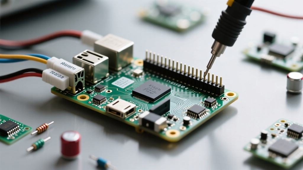
The Fix: Solder external 470 ohm pull-up resistors directly to your sensor breakout board, pulling up to the 3.3V line. Furthermore, ensure your ground return path is as short as possible. By treating the pin diagram of Raspberry Pi not just as a logical map, but as a high-frequency RF and power delivery schematic, you can push your SBC projects from hobbyist prototypes to industrial-grade deployments.