
The RP1 Southbridge: Rewiring the Raspberry Pi 5 Pinout Architecture
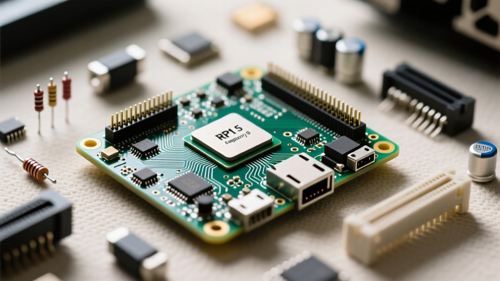
When analyzing the raspberry pi 5 pinout, enthusiasts and engineers must immediately recognize a fundamental architectural shift from previous generations. Unlike the Pi 4, where the BCM2711 SoC handled both compute and peripheral I/O, the Pi 5 utilizes a custom 28nm southbridge chip known as the RP1. This separation of duties radically alters how signals are routed to the 40-pin GPIO header and dramatically increases overall I/O throughput.
From a performance tuning perspective, the RP1 chip is a game-changer. It natively supports higher clock speeds on peripheral buses and offers additional hardware-level controllers that were previously relegated to software bit-banging. Understanding this new I/O topology is the first step in eliminating bottlenecks in high-speed data acquisition, sensor fusion, and low-latency control systems.
Exploiting the J6 PCIe Pinout for NVMe Storage Speeds
The most significant performance-oriented addition to the Pi 5 board layout is the J6 PCIe connector. This 16-pin Flexible Printed Circuit (FPC) interface exposes a single PCIe Gen 2.0 x1 lane directly from the BCM2712 SoC, bypassing the RP1 chip entirely to minimize latency.
Tuning PCIe Gen 3.0 for Maximum Throughput
By default, the Raspberry Pi 5 limits the J6 connector to PCIe Gen 2.0 speeds (roughly 5 GT/s, yielding practical throughputs around 400-800 MB/s depending on the NVMe drive and UASP overhead). However, the silicon is capable of PCIe Gen 3.0 (8 GT/s). To unlock this, you must modify the bootloader configuration. According to Jeff Geerling's extensive PCIe benchmarks, enabling Gen 3 can push sequential read speeds past 2,000 MB/s when paired with a high-end NVMe SSD like the Samsung 990 EVO or WD Black SN850X.
To enable Gen 3, add the following parameter to your /boot/firmware/config.txt file:
dtparam=pciex1_gen=3Note: While Gen 3 is officially "unsupported" due to minor signal integrity variations on the FPC trace, real-world testing shows it is highly stable for short-run NVMe HATs. Ensure your FPC cable is properly seated and shielded from EMI generated by the RP1 and main PMIC.
High-Speed Peripheral Buses: SPI and I2C Multiplexing
A common bottleneck in Pi 4 clusters and sensor arrays was I2C bus contention. The standard hardware I2C bus (I2C1 on GPIO 2 and GPIO 3) was often shared across multiple high-frequency sensors, leading to clock stretching and dropped packets. The RP1 chip solves this by exposing multiple dedicated hardware I2C and SPI controllers directly on the raspberry pi 5 pinout.
Bus Availability and Pin Mapping
| Bus Type | Pi 4 Hardware Controllers | Pi 5 (RP1) Hardware Controllers | Performance Tuning Advantage |
|---|---|---|---|
| I2C | 1 (Standard), 1 (VC) | 4 (I2C0, I2C1, I2C3, I2C4) | Isolate high-speed IMUs from slow environmental sensors to prevent bus capacitance drag. |
| SPI | 2 (SPI0, SPI1) | 3 (SPI0, SPI3, SPI4) | Dedicate SPI4 exclusively to high-bandwidth ADCs or DACs without interrupting SPI0 displays. |
| UART | 2 | 3 | Separate debug console from active GPS/LoRa telemetry streams. |
Overclocking the SPI Clock Divider
For users interfacing with high-speed ADCs (like the ADS8688) or FPGA development boards via SPI, the RP1 allows for much tighter control over the SPI clock divider. While the Pi 4 struggled to maintain stable signal integrity above 30 MHz on the GPIO header, the Pi 5's RP1 can reliably push SPI0 to 50 MHz or higher, provided you use short, shielded jumper wires and properly terminate the MISO/MOSI lines with 33-ohm series resistors to prevent ringing.
Power Delivery: Navigating the 5V/5A GPIO Constraints
Performance tuning isn't just about data throughput; it's about power stability. The Raspberry Pi Official Documentation explicitly outlines the new power requirements for the Pi 5. The board utilizes a Renesas DA9098 PMIC (Power Management Integrated Circuit), which fundamentally changes how power is distributed to the 40-pin header.
The 600mA Limit and USB-C PD Negotiation
If you power the Pi 5 with a standard 5V/3A power supply, the firmware will detect the lack of USB-C Power Delivery (PD) negotiation and impose a strict 600mA limit on the USB ports. More importantly for hardware hackers, this power state alters the current budget available on the 5V GPIO pins (Pin 2 and Pin 4). If you are driving high-performance add-ons like LED matrix HATs, heavy relay arrays, or LiDAR sensors directly from the GPIO 5V pins, a standard PSU will trigger brownouts and thermal throttling.
To guarantee the full current budget on the 5V pins and ensure stable voltage under heavy I/O loads, you must use a 27W (5V/5A) USB-C PD power supply. The official Raspberry Pi 27W PSU negotiates the 5A mode, allowing the PMIC to open the high-side FETs fully, minimizing voltage drop across the PCB traces when peripheral current draw spikes.
Debugging and UART Pinout for Boot Optimization
In headless, performance-critical deployments (such as edge-computing nodes or robotic vision systems), boot time is a critical metric. The Pi 5 retains the dedicated 3-pin JST UART debug connector (located near the J6 PCIe port), but it also maps UART0 to GPIO 14 (TX) and GPIO 15 (RX) on the main header.
By connecting a high-baud-rate USB-to-TTL serial adapter (capable of 921600 baud or higher) to the dedicated debug header, you can capture the bootloader and kernel initialization logs with microsecond precision. This allows developers to identify exactly which kernel modules or device tree overlays are causing delays in the boot sequence. Disabling unnecessary UART console output in the cmdline.txt file can shave critical milliseconds off the time-to-first-frame for Pi 5 camera setups.
Thermal Considerations for High-Density Pin Usage
As noted in the Tom's Hardware Pi 5 Review, the BCM2712 runs significantly hotter than its predecessors. When utilizing the full 40-pin header for high-speed, simultaneous data transfers (e.g., saturating the SPI and I2C buses while writing to an NVMe drive via PCIe), the RP1 and BCM2712 generate substantial localized heat.
"Signal integrity on the GPIO header degrades as ambient and PCB temperatures rise. For industrial deployments pushing the Pi 5 pinout to its absolute limits, an active cooling solution is not optional—it is a requirement for maintaining precise timing margins on high-speed digital buses."
Ensure that your enclosure design directs airflow not just over the main SoC heatsink, but across the RP1 chip and the PMIC inductor located near the USB-C port. Thermal throttling on the RP1 will silently reduce peripheral bus clocks, leading to inexplicable latency spikes in your application layer.
Summary: Tuning the Pi 5 for the Edge
The raspberry pi 5 pinout represents a mature, highly capable I/O architecture that demands a more sophisticated approach to hardware integration. By leveraging the RP1's multiple hardware buses, enabling PCIe Gen 3.0 for storage, and strictly adhering to the 5V/5A power delivery requirements, developers can transform the Pi 5 from a hobbyist tinker-board into a formidable edge-computing powerhouse.