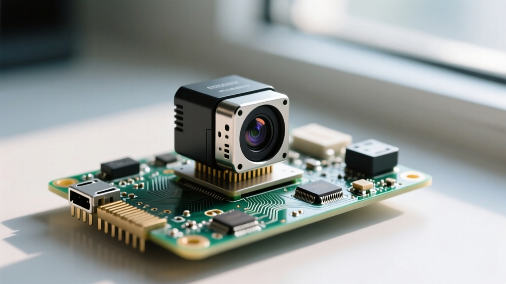
Microcontroller unit (MCU) boards are self-contained embedded computing platforms integrating a CPU core, memory subsystems, peripherals, and I/O interfaces onto a single chip or compact PCB. Unlike general-purpose computers, MCUs execute deterministic, real-time tasks with ultra-low power consumption — often drawing as little as 1.8 µA in deep-sleep mode (e.g., STM32L412KB at 3.3 V). They form the backbone of industrial sensors, medical wearables, smart home nodes, and automotive body controllers. This article details their architectural essentials: silicon-level components, timing constraints, memory mapping, peripheral integration, and quantifiable design trade-offs — grounded in datasheets from STMicroelectronics, Microchip, NXP, and Espressif. No abstractions: we cite exact clock tolerances, voltage rails, flash endurance cycles, and pin-count realities.
What Exactly Is an MCU Board?
An MCU board is not merely a 'smaller Arduino.' It is a purpose-built hardware system centered on a microcontroller IC — a complete computer-on-a-chip including processor, RAM, non-volatile program memory (Flash), and programmable peripherals. The board adds essential support circuitry: regulated power delivery (e.g., TPS63031 DC-DC converter on the Adafruit Feather M4 Express), crystal oscillators (typically 32.768 kHz for RTC + 8–48 MHz main), debug interfaces (SWD/JTAG), and physical I/O connectors. Crucially, it excludes external components required by microprocessors — no separate DRAM chips, no PCIe slots, no GPU. For example, the NXP LPC804 operates at 30 MHz, integrates 64 KB Flash, 16 KB SRAM, and runs entirely from a single 3.3 V supply without external memory.
The distinction from SoCs (Systems-on-Chip) is critical: while both integrate peripherals, MCUs maintain tight coupling between CPU and peripherals via a single bus matrix (e.g., ARM Cortex-M AHB/APB), enabling sub-microsecond interrupt latency. In contrast, SoCs like the Raspberry Pi Compute Module 4 use multi-layer interconnects, Linux OS abstraction, and external DDR4 — making them unsuitable for hard real-time control loops demanding <5 µs jitter, such as motor commutation or battery cell balancing.
Core Silicon Components
Every MCU board rests on three foundational silicon blocks: the processor core, memory subsystem, and peripheral complex. Processor cores include ARM Cortex-M0+ (e.g., RP2040 dual-core), Cortex-M4F (STM32H743 with FPU), RISC-V (GD32V103 from GigaDevice), and proprietary architectures like Microchip’s PIC18F (8-bit, 16 MB instruction cycle). Memory comprises volatile SRAM (typically 8–1024 KB), non-volatile Flash (16–2048 KB), and sometimes EEPROM (e.g., ATmega328P: 1 KB EEPROM rated for 100,000 write/erase cycles). Peripheral complexes include UART, SPI, I²C, timers, ADCs, DACs, and advanced features like USB 2.0 FS, CAN FD, or cryptographic accelerators (e.g., STM32U575’s AES-256 + PKA).
Memory Architecture: Flash, SRAM, and Memory Mapping
MCU memory is physically partitioned and mapped into fixed address spaces. Flash stores firmware and is organized in sectors (e.g., STM32G0B1: 128 KB Flash in 2 KB sectors; erase time = 20 ms/sector at 25 °C). SRAM provides runtime variables and stack space — STM32L552 offers 320 KB SRAM split across four banks (SRAM1–SRAM4), each independently configurable for retention during low-power modes. Memory-mapped I/O means peripherals reside in the same address space as RAM; writing to address 0x40000000 on an STM32 configures GPIOA’s MODER register, not memory.
Key metrics govern usability: Flash endurance is typically 10,000–100,000 erase cycles (STMicro specifies 10,000 for standard Flash, 1 million for special sectors in STM32L4+). Data retention exceeds 20 years at 55 °C. SRAM access time is sub-10 ns for Cortex-M7 parts running at 480 MHz (STM32H743). Critical applications require careful allocation: a sensor fusion algorithm using double-precision math may consume >48 KB SRAM — ruling out 32 KB devices like the nRF52832.
Flash vs. ROM vs. OTP
- Flash: Electrically erasable, reprogrammable. STM32F407 has 1 MB Flash, supports read-while-write (RWW) in dual-bank mode.
- ROM: Mask-programmed during fabrication. Used for bootloader or calibration constants. Microchip PIC16F15313 includes 2 KB ROM for factory-trimmed oscillator calibration.
- OTP (One-Time Programmable): Irreversible storage. ESP32-WROVER-B uses 1 KB OTP for MAC address and secure boot keys; write endurance = 1.
Boot configuration is hardware-defined: STM32 devices select boot source (system memory, embedded Flash, or SRAM) via BOOT0/BOOT1 pins at reset. Misconfiguration here yields a bricked device — a common field failure requiring SWD recovery.
Clock Systems and Timing Precision
MCUs rely on multiple synchronized clock domains. A typical architecture includes: (1) a low-frequency RC oscillator (32 kHz, ±50% tolerance, used for WFE/WFI wake-up), (2) a precision 32.768 kHz crystal for RTC (±20 ppm at 25 °C, e.g., Abracon AB26T), and (3) a high-frequency source — either internal RC (8 MHz ±1% on ATmega328P) or external crystal (8–25 MHz, ±10–50 ppm). The STM32L073RZ uses a 32 MHz HSE with PLL to generate 32 MHz system clock, while its LSE drives the RTC with temperature-compensated drift <±1 ppm over −40 to +85 °C.
PLLs multiply frequencies but introduce jitter. The RP2040’s PLL generates 133 MHz from a 12 MHz crystal with RMS jitter <10 ps — sufficient for USB 1.1 but marginal for Ethernet PHY clocks. Clock tree configuration is non-trivial: incorrect APB1 prescaler settings can disable USART2 on STM32F103 if PCLK1 is set below 1.25 MHz (minimum for 115200 baud at 16x oversampling).
Real-Time Constraints and Latency Budgets
Hard real-time operation demands guaranteed worst-case execution times (WCET). The Cortex-M4F’s NVIC supports up to 240 interrupt lines with programmable priority (0–255). Interrupt latency is defined as cycles from signal assertion to first instruction fetch: STM32H743 achieves 12 cycles @ 480 MHz = 25 ns. This enables 40 kHz PWM updates (25 µs period) with 100 ns resolution. Compare this to Linux-based systems where scheduling jitter exceeds 10 ms — disqualifying them for servo control.
Timer peripherals enforce timing rigor. The STM32G474’s HRTIM delivers six independent 16-bit timers with 184 ps resolution and <1 ns jitter between channels — essential for interleaved PFC converters. Missing these specs leads directly to EMI failures during EMC testing.
I/O Capabilities and Electrical Specifications
GPIO pins are not generic wires. Each exhibits defined electrical behavior per datasheet. The PIC18F47Q10 specifies VOH = 0.8 × VDD at IOL = 8 mA (high-drive mode), VOL = 0.2 × VDD at IOH = –8 mA. Exceeding these violates I²C bus specifications (standard-mode requires VOL ≤ 0.4 V at 3 mA sink). Pin multiplexing adds complexity: STM32F303K8T6 offers 25 GPIOs, but only 18 support alternate functions like SPI2_MOSI — and only 6 support analog input (ADC1_IN0–ADC1_IN5).
ESD protection is built-in but limited: most MCUs withstand ±2 kV HBM (Human Body Model), per JEDEC JS-001. Industrial designs require external TVS diodes (e.g., SMAJ5.0A) for ±8 kV contact discharge immunity. Signal integrity matters: trace lengths >5 cm for 48 MHz SPI clocks demand impedance control (50 Ω) and series termination resistors (22–33 Ω) to suppress ringing — a frequent root cause of intermittent SPI CRC errors.
| MCU Board | Max GPIO Count | ADC Resolution / Channels | UART / SPI / I²C Count | VIO Range | Pin Drive Strength |
|---|---|---|---|---|---|
| ESP32-WROOM-32 | 34 | 12-bit / 18 ch | 3 / 4 / 2 | 3.0–3.6 V | 40 mA (sink/source) |
| STM32F411RE | 50 | 12-bit / 16 ch | 4 / 3 / 3 | 1.7–3.6 V | 25 mA (max per pin) |
| nRF52840 DK | 48 | 12-bit / 8 ch | 2 / 1 / 2 | 1.7–3.6 V | 15 mA |
| MSP430FR5994 | 42 | 10-bit / 24 ch | 2 / 2 / 2 | 1.8–3.6 V | 20 mA |
| RP2040 (Pico) | 26 | 12-bit / 4 ch | 2 / 2 / 2 | 1.8–3.3 V | 50 mA (total bank) |
Power Management and Low-Power Modes
Energy efficiency defines MCU viability in battery-powered systems. The EFM32GG11B820F2048GL192 consumes 1.8 µA in EM2 (deep-sleep with RTC running) and 100 nA in EM4 (hibernate, RAM lost). Wake-up time from EM2 is 2.4 µs — fast enough for ultrasonic distance sensing at 200 Hz. Contrast with ESP32-WROVER-IB: 10 µA in light-sleep, but 150 ms wake-up latency due to RF subsystem reinitialization.
Power domains isolate functionality: STM32L5 splits VDD into VDDA (analog), VDDIO2 (I/O), and VDDCORE (CPU/SRAM). Independent regulation allows VDDA to remain at 3.3 V while VDDCORE drops to 0.95 V in low-voltage scaling mode — reducing dynamic power by 50%. Brown-out detection (BOR) thresholds are factory-trimmed: STM32G031K8 has BOR level options at 1.62 V, 2.0 V, 2.5 V, and 2.8 V — selecting 2.5 V prevents brown-out resets during Li-ion battery sag below 3.0 V.
Battery Life Calculations
Accurate runtime estimation requires weighted averaging across modes. Consider a soil moisture sensor using STM32L432KC:
- Active (64 MHz, all peripherals): 82 µA/MHz → 5.25 mA
- Sleep (all clocks off, RTC active): 1.2 µA
- Measurement cycle: 1 s active + 59 s sleep
- Average current = (5.25 mA × 1 + 0.0012 mA × 59) / 60 = 87.7 µA
- With 2000 mAh CR123A battery: 2000 / 0.0877 ≈ 22,800 hours ≈ 2.6 years
Omitting sleep-mode leakage or temperature derating (−40 °C increases leakage 3×) causes field failures.
Debugging, Programming, and Development Infrastructure
Production-grade MCU boards mandate robust debug access. SWD (Serial Wire Debug) is the de facto standard: two pins (SWDIO, SWCLK), 4-pin connector (add GND, VTARGET). ST-Link/V2-1 on Nucleo boards supports SWD speeds up to 4 MHz and full memory read/write, breakpoint, and watchpoint debugging. JTAG remains necessary for boundary-scan testing (IEEE 1149.1) on dense PCBs with >100 pins.
Programming methods vary: mass-production uses SWD via J-Link PRO ($599) for 100+ units/hour; hobbyists use USB-CDC bootloaders (e.g., RP2040’s UF2 mode). Security-critical apps disable debug ports permanently — STM32L5 fuses allow irreversible debug lock after programming, preventing firmware extraction via SWD.
Toolchain maturity affects development velocity. ARM GCC 12.2 supports Cortex-M85 with -O3 optimization yielding 1.8x code density improvement over GCC 9.2. Keil MDK-ARM v5.38 reduces vector table initialization time by 42% versus v5.26 — measurable in boot-time-critical applications like aircraft black boxes.
Selecting the Right MCU Board: Decision Framework
Selection must begin with quantifiable requirements, not brand preference. Use this hierarchy:
- Real-time deadline: If loop time < 10 µs, eliminate Cortex-M0/M0+; choose Cortex-M4F or M7 with cache and TCM (Tightly Coupled Memory).
- Power budget: For >10-year coin-cell life, target sub-µA deep-sleep (EFM32, MSP430FR, STM32L5).
- Analog fidelity: 16-bit ADC needed? Only ADuCM3029 (Analog Devices) and STM32H7 offer true 16-bit SAR with <1 LSB INL.
- Peripheral concurrency: Need simultaneous USB + Ethernet + SDIO? Only i.MX RT1064 (NXP) or RA6M5 (Renesas) deliver full-speed USB HS + 100 Mbps Ethernet MAC + SDHC controller.
- Certification: Medical (IEC 62304) or automotive (ISO 26262 ASIL-B) mandates specific failure-in-time (FIT) rates. Microchip’s SAMV71Q21 reports FIT = 120 at 105 °C — validated per JEDEC JEP148.
Cost-per-unit at volume is decisive: ATSAMD21G18A costs $1.42 @ 10k units (Digi-Key, June 2024), while the equivalent STM32G071KBT6 is $1.28 — a 9.2% saving that scales to $128,000 annually on 1M units. However, toolchain licensing (IAR Embedded Workbench $3,490/year) may offset silicon savings.
Thermal management is often overlooked. The STM32H743ITR dissipates 0.8 W at 480 MHz in ambient 60 °C. Its 144-pin LQFP package has θJA = 32 °C/W — junction temperature = 60 + (0.8 × 32) = 85.6 °C, within spec. Add 10 °C margin for enclosure heating: max ambient = 75.6 °C. Without thermal calculation, field failures occur above 85 °C ambient.
Finally, longevity matters. Microchip guarantees 15-year product availability for PIC18F67K40; STMicro extends STM32F030F4P6 to 2030. Avoid ‘new’ parts with unproven supply chains — the ESP32-S2 faced 26-week lead times in Q3 2022, halting production for three OEMs.
MCU board selection is engineering, not shopping. It demands cross-referencing datasheets, calculating worst-case power, validating timing paths, and verifying supply-chain resilience. There are no shortcuts — only specifications, measurements, and consequences.
When evaluating the Adafruit Metro M4 (ATSAMD51J19), note its 192 KB SRAM enables real-time FFT on 1024-point audio buffers — impossible on the 32 KB SAMD21. When choosing between NXP’s KL27Z and K32L2B, the latter’s 256 KB Flash and CAN FD support justify its $0.22 higher BOM cost for telematics gateways. Every specification has a physical consequence: voltage tolerance dictates regulator choice; pin count determines PCB layer count; clock jitter defines EMI filter complexity.
Engineers who treat MCU boards as black boxes ship products that fail certification, drain batteries in weeks, or miss deadlines under load. Those who master the essentials — Flash sector timing, GPIO drive limits, PLL jitter budgets, and thermal resistance — build systems that operate reliably for a decade. The data is public. The discipline is yours.