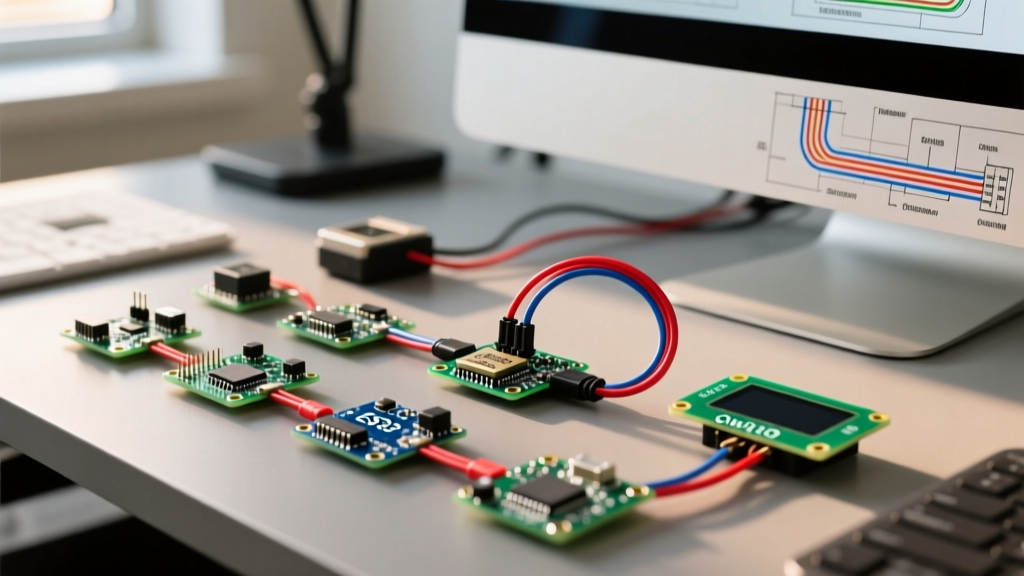

For embedded engineers and hobbyists alike, the transition from a conceptual schematic to a working physical prototype is often bottlenecked by a single, frustrating variable: wiring. Traditional I2C prototyping on breadboards requires a tangled web of jumper wires, manual pull-up resistor calculations, and constant debugging of crossed SDA and SCL lines. In 2026, with the maker market heavily favoring native 3.3V architectures like the Arduino Nano ESP32 and Seeed Studio XIAO series, the industry has largely standardized around modular I2C ecosystems. In maker communities, this is often colloquially searched as the Arduino Q system, referring specifically to the SparkFun Qwiic connect standard and its Adafruit STEMMA QT counterpart.
Adopting this standardized 4-pin JST-SH workflow eliminates soldering during the R&D phase, reduces wiring errors to near zero, and dramatically accelerates iteration cycles. This guide provides a deep-dive, expert-level workflow optimization strategy for mastering the Qwiic ecosystem, addressing the hidden electrical pitfalls that cause I2C bus failures in complex sensor arrays.
Decoding the Hardware Standard
The foundation of this workflow optimization is the physical connector. Both SparkFun's Qwiic and Adafruit's STEMMA QT utilize the 4-pin JST-SH connector with a 1.0mm pitch. This is a critical distinction from the older, larger 2.0mm pitch JST-PH connectors used for LiPo batteries. The 1.0mm pitch keeps the footprint compact, allowing multiple sensor breakouts to remain under 1 square inch.
Standardized Pinout Matrix
Unlike raw I2C headers where pin order can vary wildly between manufacturers, the Qwiic standard enforces a strict, universal pinout. Reversing a cable simply flips the GND and 3.3V pins, which, while potentially dangerous for raw components, is mitigated by the polarized nature of the JST-SH housing.
| Pin Number | Function | Wire Color (Standard) | Voltage Level |
|---|---|---|---|
| 1 | GND | Black | 0V Reference |
| 2 | 3.3V Power | Red | 3.3V (Max 500mA total bus) |
| 3 | SDA (Data) | Blue | 3.3V Logic |
| 4 | SCL (Clock) | Yellow | 3.3V Logic |
For comprehensive hardware specifications and compatible breakout boards, engineers should consult the official SparkFun Qwiic Connect System documentation, which maintains an updated registry of all supported I2C addresses and power draw metrics.
Workflow Bottleneck 1: The Pull-Up Resistor Trap
The most common cause of I2C failure in a daisy-chained Qwiic workflow is not a software bug, but a hardware electrical fault related to pull-up resistors. The I2C specification requires open-drain lines pulled high to the logic voltage. Most Qwiic breakout boards ship with 4.7kΩ pull-up resistors enabled via a solder jumper on the PCB.
The Math Behind the Failure
When you daisy-chain multiple boards, these pull-up resistors are placed in parallel. The equivalent resistance drops according to the formula:
R_total = 1 / (1/R_1 + 1/R_2 + ... + 1/R_n)
- 1 Board: 4.7kΩ (Optimal)
- 2 Boards: 2.35kΩ (Acceptable)
- 3 Boards: 1.56kΩ (Marginal)
- 4 Boards: 1.17kΩ (Critical Failure Zone)
When the total pull-up resistance drops below 2kΩ, the I2C master (e.g., your Arduino Nano ESP32) must sink a significantly higher current to pull the SDA/SCL lines LOW. If the master's internal transistor cannot sink enough current to pull the voltage below the V_IL (Voltage Input Low) threshold of 0.4V, the slave sensors will fail to register the LOW state, resulting in I2C NACK errors and bus lockups.
Expert Workflow Tip: Before assembling a multi-sensor Qwiic array, use an X-Acto knife to sever the I2C pull-up jumper on all but the primary master board or the first sensor in the chain. Verify the severing with a multimeter in continuity mode. This single step resolves over 80% of unexplained I2C communication drops in complex prototypes.
Workflow Bottleneck 2: Bus Capacitance and Cable Length
While Qwiic cables make physical connections trivial, they introduce parasitic capacitance. According to the official NXP I2C-bus specification (UM10204), standard-mode I2C (100kHz) and fast-mode I2C (400kHz) are limited to a maximum bus capacitance of 400pF.
A standard 100mm Qwiic cable adds approximately 15pF to 20pF of capacitance to the bus. If you are chaining five sensors using 200mm cables, your cable capacitance alone approaches 200pF. Add the inherent capacitance of the sensor ICs and the microcontroller pins, and you can easily breach the 400pF limit. When this happens, the RC time constant of the bus increases, rounding off the sharp square-wave edges of the I2C clock signal into slow, sloping curves, leading to data corruption.
Optimization Strategies for Long Runs
- Consolidate Cable Lengths: Use 50mm cables for tightly clustered sensors and reserve 500mm cables only for the final node in the chain.
- Drop the Clock Speed: If your sensor array requires long cable runs, force the Arduino Wire library to operate at 100kHz (Standard Mode) rather than 400kHz. In your sketch setup, use
Wire.setClock(100000);to give the signal more time to reach the high-voltage threshold. - Deploy Active Extenders: For industrial or large-scale art installations requiring runs over 2 meters, integrate an active I2C bus extender like the NXP PCA9615. This chip converts the I2C signals into differential signals, allowing them to travel over standard CAT5 Ethernet cable for up to 30 meters without capacitance degradation.
Time vs. Cost Analysis: Traditional vs. Modular I2C
Transitioning to a modular I2C workflow requires an upfront capital investment in cables and specialized breakouts. However, when calculating the engineering cost of debugging time, the ROI is immediate. Below is a comparative matrix based on a standard 5-sensor environmental monitoring prototype.
| Metric | Traditional Breadboard & Jumpers | Qwiic / STEMMA QT Ecosystem |
|---|---|---|
| Hardware Cost (Sensors) | ~$45 (Raw ICs or generic modules) | ~$85 (Integrated Qwiic breakouts) |
| Wiring Materials | $5 (Jumper wires, 4.7k resistors) | $12 (Five 100mm Qwiic cables) |
| Assembly Time | 45 - 60 minutes | 3 - 5 minutes |
| Debugging Time (I2C Faults) | 2 - 4 hours (Tracing crossed wires) | 10 minutes (Checking pull-up jumpers) |
| Reliability (Vibration/Movement) | Poor (Breadboard contacts oxidize/loosen) | Excellent (Friction-locked JST-SH) |
Voltage Translation: Bridging the 5V Legacy Gap
As of 2026, the vast majority of modern maker boards (Arduino Nano ESP32, Adafruit QT Py ESP32-S3) operate at native 3.3V logic, perfectly aligning with the Qwiic standard. However, legacy 5V boards like the Arduino Uno R3 or Mega 2560 are still prevalent in educational and legacy industrial settings.
Connecting 3.3V Qwiic sensors directly to a 5V SDA/SCL line will degrade the sensor's internal protection diodes over time, leading to premature silicon failure. To optimize your workflow when mixing voltage domains, utilize a dedicated Qwiic logic level converter. SparkFun's Qwiic Level Shifter utilizes BSS138 MOSFETs to safely translate the 3.3V sensor lines to 5V for the master microcontroller, ensuring bidirectional communication without signal clipping.
Transitioning from Prototype to Production
The ultimate strength of the modular I2C workflow is how seamlessly it translates to custom PCB manufacturing. Once your firmware is validated and your sensor array is finalized, you do not need to redesign your I2C bus topology. Modern EDA software like KiCad 8 includes native JST-SH 1.0mm footprints (such as the SM04B-SRSS-TB).
For low-volume production runs (10 to 50 units), designing a custom "backplane" PCB with female JST-SH connectors and integrated pull-up resistors allows you to snap your off-the-shelf Qwiic sensors directly into a finalized product enclosure. For high-volume scaling (10,000+ units), you simply copy the schematic blocks of the specific sensors directly onto your main microcontroller PCB, dropping the connectors entirely to save on BOM costs. For further insights on scaling modular sensor networks, the Adafruit STEMMA QT design guide offers excellent schematic references for integrating these footprints into custom silicon layouts.
Summary Checklist for Flawless I2C Workflows
To ensure your next microcontroller project avoids the common pitfalls of I2C bus design, run through this pre-flight checklist:
- Verify all boards are native 3.3V or properly level-shifted.
- Cut the pull-up solder jumpers on all secondary slave nodes.
- Calculate total bus capacitance if using more than three 200mm cables.
- Run an I2C scanner sketch (
Wire.h) to verify all hex addresses before writing application logic. - Use a digital oscilloscope to inspect SDA/SCL edge rise times if operating at 400kHz Fast Mode.
By treating physical connectivity as a standardized system rather than an ad-hoc afterthought, embedded developers can reclaim dozens of hours previously lost to hardware debugging, focusing entirely on firmware optimization and product innovation.