
The ATmega2560 Core: Why Pin Mapping Matters
When makers outgrow the limitations of the standard Uno, the Arduino Mega 2560 is the inevitable next step. Whether you are building a multi-axis CNC router, a complex 3D printer control board, or an advanced environmental monitoring station, the sheer I/O density of the Mega is unmatched in the hobbyist space. However, understanding the arduino pinout mega layout is critical. Unlike smaller boards, the Mega routes its communication buses and timer-bound PWM pins differently, leading to severe compatibility issues if you blindly port code or stack shields designed for the ATmega328P.
In this comprehensive compatibility guide, we break down the exact pin mappings, voltage tolerances, and shield relocation traps you need to know to deploy the Mega 2560 successfully in 2026. We will also cover the thermal limitations of the onboard voltage regulators, ensuring your high-current projects do not end in silicon failure.
Comprehensive Arduino Pinout Mega Mapping Table
The official Arduino Mega 2560 Rev3 features 54 digital input/output pins and 16 analog inputs. Below is the master reference table for bus allocations and alternate functions.
| Function Category | Pins | Notes & Constraints |
|---|---|---|
| Digital I/O | 0 to 53 | 54 total pins; all can be used as standard GPIO. |
| Analog Inputs | A0 to A15 | 16 channels, 10-bit ADC resolution (0-1023). |
| PWM Outputs | 2-13, 44-46 | 15 pins total. Hardware timers drive these; no software overhead. |
| Hardware UART (Serial) | 0/1, 14/15, 16/17, 18/19 | 4 independent serial ports (Serial, Serial1, Serial2, Serial3). |
| SPI Bus | 50(MISO), 51(MOSI), 52(SCK), 53(SS) | Also mirrored on the 2x3 ICSP header. |
| I2C / TWI Bus | 20 (SDA), 21 (SCL) | Supports 100kHz and 400kHz Fast Mode. |
| External Interrupts | 2, 3, 18, 19, 20, 21 | INT0 to INT5. Crucial for rotary encoders and flow sensors. |
Digital, PWM, and Analog Breakdown
A common misconception is that all digital pins on the Mega support hardware PWM. They do not. Only pins 2 through 13 and 44 through 46 are connected to the internal hardware timers of the ATmega2560. If you attempt to use analogWrite() on pin 24, for example, the microcontroller will simply output a digital HIGH if the value is above 127, or LOW if below, rather than generating a pulse-width modulated square wave. For projects requiring extensive motor control or LED dimming, you must plan your wiring around these specific 15 PWM-capable pins.
Shield Compatibility: Where Uno Shields Fail on the Mega
The physical footprint of the Mega 2560 maintains the same 1.1-inch spacing for the primary digital and analog headers as the Uno, meaning most shields will physically plug in. However, electrical compatibility is a different story. According to the official Arduino hardware documentation, the routing of the SPI and I2C buses was changed to accommodate the larger 100-pin TQFP package of the ATmega2560.
The SPI Bus Relocation Problem
On the Uno, the SPI bus (used for SD cards, RFID readers, and TFT displays) resides on pins 11 (MOSI), 12 (MISO), and 13 (SCK). On the Mega, these pins are relocated to 51 (MOSI), 50 (MISO), and 52 (SCK). If you plug an older Uno Ethernet shield or SD card module directly into the Mega's digital headers, it will not communicate.
The Solution: Modern shields route SPI through the 2x3 ICSP header, which is identically placed on both the Uno and Mega. If you are using a legacy shield or raw jumper wires, you must manually route SPI to pins 50-53. Pin 53 serves as the default Hardware Slave Select (SS) pin; it must be kept as an OUTPUT, or the SPI controller will automatically drop into slave mode, causing total bus failure.
The I2C Bus Relocation
Similarly, the I2C bus (used for OLEDs, IMUs, and RTC modules) moved from the analog pins (A4/A5 on the Uno) to dedicated digital pins 20 (SDA) and 21 (SCL) on the Mega. While the Rev3 board added duplicate SDA/SCL pins next to the AREF pin for newer shield compatibility, raw wiring requires you to target pins 20 and 21. Attempting to scan the I2C bus on A4/A5 using the standard Wire library on a Mega will yield zero results.
Power Delivery and Voltage Logic Limits
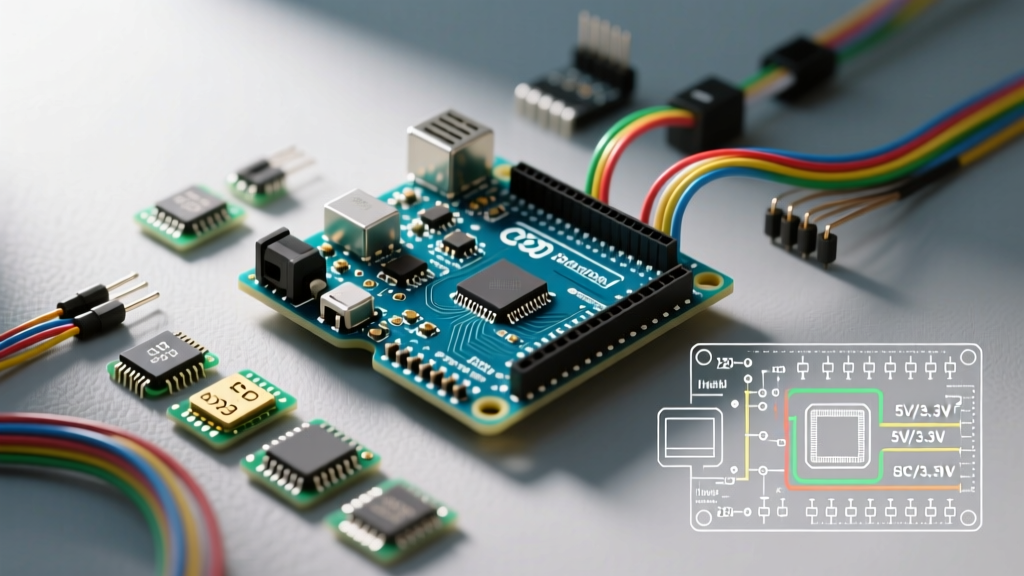
Understanding the power architecture is just as vital as the signal pinout. The Mega 2560 Rev3 operates at 5V logic. Supplying 3.3V signals directly into 5V tolerant inputs is generally safe, but connecting 5V outputs to 3.3V sensors (like the BME280 or ESP32) will destroy the sensor's silicon.
CRITICAL WARNING: Never connect 5V Mega I/O pins directly to 3.3V logic devices without a bidirectional logic level shifter. As detailed in SparkFun's guide on logic levels, exceeding the VCC + 0.5V threshold on a 3.3V chip triggers internal protection diodes, leading to thermal runaway and permanent component death.
Regulator Thermal Constraints
The board features an NCP1117ST50T3G linear regulator for the 5V rail and an LP2985 for the 3.3V rail. The 3.3V pin can safely supply up to 150mA, which is sufficient for most modern low-power sensors but inadequate for high-draw RF modules like the nRF24L01+ without an external capacitor or dedicated 3.3V buck converter.
When powering the board via the barrel jack (Vin), the 5V regulator must dissipate the voltage difference as heat. If you supply 12V to the jack and draw 400mA from the 5V pin, the regulator dissipates 2.8 Watts. The SOT-223 package will hit thermal shutdown at approximately 150°C junction temperature. For high-current 5V peripherals (servos, LED strips), bypass the onboard regulator entirely and inject 5V directly into the 5V header pin, ensuring your external power supply shares a common ground with the Mega.
Real-World Failure Modes and Edge Cases
Based on field deployments and teardowns, here are the most common wiring and configuration failures associated with the Mega 2560 pinout:
- Backpowering via USB and Vin: If you connect a 12V supply to Vin while simultaneously connected to a PC via USB, the onboard polyfuse and protection diodes can overheat if the external supply bleeds backward. Always use a USB cable with the 5V line severed for high-voltage Vin debugging.
- Exceeding Per-Pin Current: The Microchip ATmega2560 datasheet specifies an absolute maximum of 40mA per I/O pin, with a total package limit of 200mA for all VCC/GND pins combined. Driving multiple 20mA relays directly from GPIO pins will degrade the microcontroller's bond wires over time. Always use MOSFETs or optocouplers for inductive loads.
- Analog Reference Drift: When using precision analog sensors on pins A0-A15, relying on the default 5V USB reference introduces noise. Use the AREF pin with a clean 2.5V or 4.096V external voltage reference and call
analogReference(EXTERNAL)in your setup loop to stabilize ADC readings. - CH340G Clone Latency: Budget clones (priced around $14-$18 in 2026) often replace the ATmega16U2 USB-to-Serial chip with a CH340G. While pin-compatible for standard uploads, the CH340G can introduce timing jitter on Serial0 (pins 0 and 1) during high-baud-rate (1Mbps+) data streaming. For high-speed telemetry, use Serial1 (pins 18/19) with a dedicated FTDI adapter.
Frequently Asked Questions
Can I use an Uno motor shield on the Mega 2560?
Yes, but with caveats. The Arduino Motor Shield Rev3 routes direction and PWM pins to standard digital I/O (pins 3, 11, 12, 13). Since pins 11, 12, and 13 are not SPI on the Mega, the shield works perfectly for motor control. However, if the shield uses pins 11-13 for SPI communication (like older Ethernet shields), it will fail unless modified with jumper wires to route SPI to pins 50-52.
How many hardware serial ports does the Mega have?
The Mega features four hardware UARTs. Serial (Pins 0/1) is shared with the USB interface. Serial1 (Pins 18/19), Serial2 (Pins 16/17), and Serial3 (Pins 14/15) are completely independent, allowing you to simultaneously communicate with a GPS module, a cellular modem, and a secondary microcontroller without software serial bottlenecks.
What is the maximum voltage I can apply to the Vin pin?
The absolute maximum rating for the Vin pin is 12V. While the board might technically survive 15V, the NCP1117 regulator will enter thermal shutdown almost immediately under any meaningful load. For optimal thermal performance and efficiency, supply the Vin pin with exactly 7.5V to 9V.