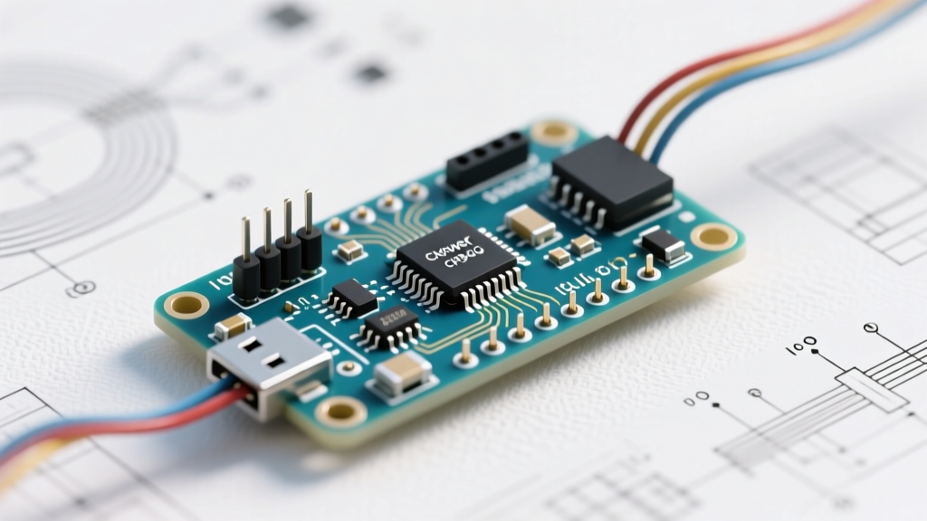

Whether you are designing a custom printed circuit board (PCB) or troubleshooting a bricked development board, understanding the Arduino Nano schematic is a non-negotiable skill for embedded systems engineers. While the Nano remains one of the most popular microcontroller platforms in 2026 due to its compact 18x45mm footprint, its dense layout hides several critical circuit design choices that can make or break a project.
In this feature deep dive, we dissect the official and clone schematics of the classic Arduino Nano (ATmega328P variant). We will analyze the power delivery network (PDN), the USB-to-serial translation architectures, and the I/O protection mechanisms, providing you with the exact data needed to transition from a breadboard prototype to a production-ready schematic.
The Microcontroller Core: ATmega328P-AU
At the heart of the classic Nano schematic sits the Microchip ATmega328P-AU, housed in a 32-lead TQFP package. Unlike the DIP-28 package found on the Arduino Uno, the surface-mount TQFP variant exposes two additional analog pins (ADC6 and ADC7), bringing the total analog inputs to eight. However, these specific pins are strictly analog inputs; they lack internal digital pull-up resistors and cannot be used as digital I/O or PWM outputs.
When reviewing the schematic, pay close attention to the decoupling network. The ATmega328P-AU requires a 100nF ceramic capacitor on every VCC and AVCC pin, placed as physically close to the IC pads as possible. In custom PCB translations of the Nano schematic, omitting the AVCC decoupling capacitor (often designated as C12 or C14 depending on the revision) is a primary cause of erratic ADC readings and noisy sensor data.
Power Delivery Network (PDN): 5V, 3.3V, and VIN
The power regulation circuit is where the official Arduino Nano schematic diverges drastically from the cheap clones flooding the market. Understanding these differences is critical when calculating your project's power budget.
The 5V Rail and VIN Regulation
The Nano can be powered via the USB Mini-B connector (5V) or the VIN pin. The schematic utilizes a power multiplexing circuit to prevent backfeeding. When powered via VIN (recommended 7V to 12V), the voltage passes through a linear regulator. The official boards historically used an MC33269 or similar LDO, while modern 2026 clones almost universally use the AMS1117-5.0. Keep in mind that linear regulators dissipate excess voltage as heat; feeding 12V into VIN while drawing 200mA from the 5V pin will cause the regulator to overheat and trigger thermal shutdown.
The 3.3V Pin Trap: 50mA vs. 800mA
This is the most common pitfall for engineers reading the Nano schematic. On the official board, the 3.3V pin is not powered by a dedicated voltage regulator. Instead, it is tied directly to the internal 3.3V LDO of the USB interface chip (the FT232RL). This internal regulator has a strict maximum current limit of 50mA. Attempting to power an ESP8266 Wi-Fi module or an NRF24L01 radio directly from the official Nano's 3.3V pin will result in immediate brownouts.
Conversely, most CH340G-based clones include a dedicated AMS1117-3.3 LDO on the PCB, capable of sourcing up to 800mA. Always verify which schematic your specific board adheres to before attaching high-current 3.3V peripherals.
USB-to-Serial Translation: FT232RL vs. CH340G
The USB interface circuit handles serial communication and provides the DTR (Data Terminal Ready) signal required for auto-resetting the microcontroller during firmware uploads.
- Official Schematic (FT232RL): The FTDI FT232RL is a robust, highly integrated USB-to-serial bridge. It requires a 6MHz external crystal oscillator and an external EEPROM (usually a 93C46) to store USB VID/PID descriptors. This adds roughly $4.50 to the component BOM cost.
- Clone Schematic (CH340G): The WCH CH340G dominates the 2026 clone market due to its $0.30 price point. The schematic for the CH340G requires a 12MHz crystal oscillator and lacks an external EEPROM, relying on hardcoded internal USB descriptors. It also requires a specific driver installation on older operating systems, though Windows 11 and modern Linux kernels include native support.
Critical Schematic Reference Designators
When troubleshooting or modifying the board, use this cross-reference table to locate key components on the silkscreen and schematic:
| Designator | Component | Function | Common Failure Mode |
|---|---|---|---|
| U1 | ATmega328P-AU | Main Microcontroller | Shorted I/O pins due to overvoltage |
| U2 | FT232RL / CH340G | USB-to-Serial Bridge | ESD damage from ungrounded USB cables |
| U3 | AMS1117-5.0 / LDO | VIN to 5V Regulator | Thermal shutdown from high VIN voltage |
| Y1 | 16MHz Crystal | MCU System Clock | Physical cracking from mechanical shock |
| Y2 | 6MHz / 12MHz Crystal | USB IC Clock | USB enumeration failure |
| C1 | 100nF Capacitor | Reset Line Filter | Spurious resets in high-EMI environments |
The Auto-Reset Circuit Explained
Unlike older boards that required a manual button press to enter the bootloader, the Nano schematic implements an elegant auto-reset mechanism. The DTR line from the USB-to-serial IC is routed through a 100nF capacitor (usually designated as C1 or C18) to the RESET pin of the ATmega328P. The RESET pin is also tied to the 5V rail via a 10kΩ pull-up resistor.
When the Arduino IDE initiates an upload, the USB IC pulls the DTR line low. The 100nF capacitor acts as a differentiator, creating a brief negative voltage spike on the RESET pin, effectively pulling it below the logic-low threshold for just long enough to trigger the bootloader. If your board uploads successfully but immediately restarts upon opening the Serial Monitor, this 100nF capacitor has likely failed short, holding the MCU in a perpetual reset state whenever the serial port is opened.
I/O Protection and Current Sinking Limits
The ATmega328P schematic reveals internal clamping diodes on every I/O pin, routing to VCC and GND. These diodes are designed to protect against high-frequency transients, not continuous overvoltage. If you apply 6V to a 5V-tolerant I/O pin, the internal diode will conduct, attempting to clamp the voltage to VCC + 0.5V. This will rapidly destroy the silicon trace inside the IC.
Furthermore, while the absolute maximum rating per I/O pin is 40mA, the official Arduino Nano documentation and Microchip datasheets recommend keeping continuous current below 20mA per pin. More importantly, the cumulative current sourced or sunk across all I/O ports must not exceed 200mA. Driving multiple high-current LEDs or relays directly from the Nano's I/O pins without external MOSFETs or ULN2803 Darlington arrays will lead to ground bounce, logic errors, and eventual MCU death.
Translating the Schematic to a Custom PCB
When migrating from a Nano-on-a-breadboard to a custom PCB, you do not need to copy the entire schematic. To reduce BOM costs and board space in 2026 production runs, strip away the USB-to-serial circuit (U2), the USB connector, and the VIN linear regulator. Instead, design your custom board to accept a programmed ATmega328P-AU, utilizing a 6-pin ICSP header for firmware updates via an external programmer (like a USBasp or Pololu AVR ISP). This removes the $5+ USB IC and associated passives, leaving only the core MCU, a 16MHz crystal, the 16-pin ISP header, and the necessary 100nF decoupling network.
Expert Troubleshooting Tip: If a Nano is completely dead and draws 0mA from USB, check the polyfuse (often marked as 'P' or '501' on the silkscreen) located near the USB connector. While rare, a shorted downstream capacitor can trip this resettable fuse. If the polyfuse is intact but the 5V rail reads 0V, the USB Mini-B connector's solder joints have likely fractured from mechanical stress—a common failure point requiring a quick reflow with a hot air station.
Mastering the Arduino Nano schematic transforms you from a module-swapper into a true embedded hardware designer. By understanding the exact current limits of the 3.3V rail, the nuances of the auto-reset capacitor, and the thermal realities of the VIN regulator, you can design robust, fail-safe electronics that survive long past the prototyping phase.