
The Translation Gap: Logic vs. Geography
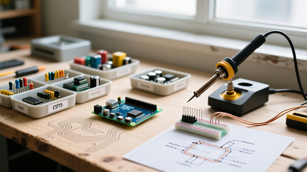
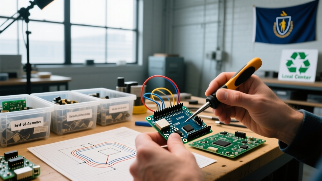
For every electronics beginner, there comes a critical moment of friction: staring at a beautifully clean schematic and then looking down at a chaotic, tangled mess of jumper wires on a solderless prototyping board. A breadboard circuit diagram is not a single standardized document; rather, it is the conceptual bridge between a logical schematic and a physical layout. While a schematic represents electrical relationships logically, a breadboard forces you to think geographically. Understanding how to translate abstract symbols into physical node connections is the most vital skill in early electronics prototyping.
According to Adafruit's Guide to Reading Schematics, a schematic is a map of electrical connections, not physical placement. When you attempt to build a physical breadboard circuit diagram layout, you must mentally reorganize that map to fit the rigid, physical constraints of the breadboard's internal copper spring clips. This guide will teach you the exact methodology to bridge this gap, ensuring your prototypes power on correctly the very first time.
Decoding the Solderless Grid Matrix
Before you can translate a schematic, you must intimately understand the physical medium. A standard 830-point solderless breadboard (like the industry-standard Elenco Model 9425) is divided into specific functional zones.
Terminal Strips and the DIP Trench
The main working area consists of terminal strips arranged in rows of five holes (a, b, c, d, e and f, g, h, i, j). Underneath the plastic housing, metal spring clips connect these five holes electrically. The central trench (the DIP trench) physically separates the left and right sides, providing exactly 0.6 inches of clearance. This specific width is designed to straddle Dual In-line Package (DIP) integrated circuits, ensuring that pin 1 and pin 2 do not short together. Placing an IC anywhere else on the board guarantees an immediate short circuit between adjacent pins.
Power Bussing and Contact Resistance
The outer rails (marked with red and blue lines) run vertically across the entire length of the board. These are your power and ground buses. However, beginners often forget that breadboards have inherent contact resistance, typically ranging from 10 to 50 milliohms per connection point. While negligible for logic signals, this resistance can cause significant voltage drops in high-current paths, such as motor driver circuits. Always use the power rails for VCC and GND, and never route high-current loads (above 1 Amp) directly through the breadboard's internal clips.
The 4-Step Translation Protocol
Translating a schematic into a breadboard circuit diagram layout requires a strict, repeatable sequence. Abandoning this sequence is the primary cause of the dreaded "rat's nest" wiring.
Step 1: Anchor the Silicon
Always begin by placing your active components—Integrated Circuits (ICs), transistors, and optocouplers. Place DIP ICs across the center trench. Orient them correctly by locating the notch or dot indicating Pin 1. Once the ICs are anchored, they dictate the physical constraints for the rest of the circuit. Do not place passive components yet.
Step 2: Establish the DC Bussing
Next, route your power. Use red jumper wires to connect your positive voltage source to the red (+) rails, and black wires for ground to the blue (-) rails. If your circuit requires multiple voltage domains (e.g., 5V for logic and 12V for actuators), use the split power rails on opposite sides of the board and label them with masking tape. Add decoupling capacitors (typically 100nF ceramic) directly across the VCC and GND pins of every IC at this stage to suppress high-frequency noise.
Step 3: Route the Signal Topology
With power established, move to the signal routing. Translate the schematic node-by-node. Instead of trying to match the physical placement of resistors and capacitors to the schematic drawing, optimize for the shortest possible wire runs. Use the unused holes in the IC's terminal strip to connect passive components directly to the IC pins, minimizing the need for long jumper wires.
Step 4: The Continuity Audit
Before applying power, grab a digital multimeter (DMM). Set it to continuity mode and verify that your VCC and GND rails are not shorted. Check the voltage at the furthest point of your power rails to ensure there is no unintended voltage drop.
Component Placement Matrix
To streamline your translation process, refer to this decision matrix when moving from schematic to physical layout:
| Component Type | Schematic Symbol | Breadboard Placement Strategy | Common Beginner Pitfall |
|---|---|---|---|
| DIP ICs (e.g., 555, 74HC595) | Rectangle with numbered pins | Straddle the center trench; orient Pin 1 top-left | Placing entirely on one side, shorting adjacent pins |
| Electrolytic Capacitors | Polarized parallel lines | Place near power entry points; observe polarity stripe | Reversing polarity, causing dielectric breakdown |
| Resistors | Zig-zag line | Bend leads to fit terminal strips; use as signal bridges | Trimming leads too short to reach adjacent rows |
| Transistors (e.g., 2N2222) | Circle with B, C, E arrows | Align flat face to match schematic pinout (E-B-C) | Assuming pinout matches physical left-to-right order |
Avoiding the Rat's Nest: Pro Routing Techniques
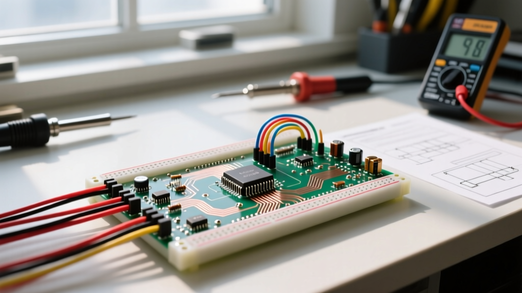
A clean breadboard circuit diagram layout is not just about aesthetics; it is crucial for debugging. When a circuit fails, you must be able to trace the signal path visually.
- Strict Color Coding: Red is strictly for VCC (positive). Black is strictly for GND. Use yellow, orange, or green for signal lines. Never mix these conventions, even if you run out of wire colors mid-build. Stop and strip more wire.
- Wire Stripping Precision: The ideal exposed wire length for a standard solderless breadboard is exactly 6mm (1/4 inch). If you strip 12mm, the exposed copper can easily brush against an adjacent row, causing an intermittent short. Invest in a precision wire stripper like the Hakko CHP 20-SE, which is calibrated for 22 AWG solid core wire.
- Use 22 AWG Solid Core Wire: Stranded wire will fray and jam the internal spring clips. Always use 22 AWG solid copper wire for jumper connections. It is the exact diameter required to engage the breadboard's internal contacts securely without permanently deforming them.
"A well-routed breadboard should look like a city grid, not a bowl of spaghetti. Right angles and flat-lying wires are the hallmarks of a professional prototype." — SparkFun's Breadboard Tutorial
Troubleshooting Ghost Voltages and Parasitics
Even with a perfect breadboard circuit diagram translation, physical prototyping introduces real-world anomalies that schematics ignore.
Parasitic Capacitance
The internal metal strips of a breadboard run parallel to each other, creating a parasitic capacitor between adjacent rows. This capacitance is typically around 2pF to 5pF. While irrelevant for DC circuits or low-frequency audio, this parasitic capacitance can cause high-frequency oscillation in RF circuits or fast-switching digital logic (like SPI or I2C buses running above 1MHz). If your digital signals show ringing on an oscilloscope, try moving the sensitive signal lines to opposite sides of the DIP trench to minimize capacitive coupling.
Floating CMOS Inputs
A classic beginner mistake is leaving unused input pins on CMOS logic chips (like the 74HC series) disconnected. According to digital logic design principles outlined by All About Circuits, a floating CMOS input acts as a high-impedance antenna. It will pick up ambient electromagnetic interference, causing the internal MOSFETs to rapidly switch on and off. This leads to excessive current draw, overheating the IC, and introducing massive noise into your power rails. Always tie unused CMOS inputs to either VCC or GND via a pull-up or pull-down resistor.
Essential Prototyping Gear
To execute these techniques flawlessly, your toolkit must be up to par. Skip the cheap, off-brand kits and invest in reliable prototyping foundations:
- Elenco Model 9425 Breadboard: Features nickel-silver plated contacts for lower resistance and longer lifespan compared to standard tin-plated clones.
- Hakko CHP 20-SE Wire Strippers: Flush-cut precision strippers that prevent nicking the copper core of 22 AWG wire.
- Pre-formed Jumper Wire Kits: While making your own jumpers is best for custom lengths, having a kit of pre-bent, varying-length solid jumpers (like those from Bus Pirate or SparkFun) saves hours of tedious bending.
- Benchtop Power Supply: Avoid relying solely on 9V batteries or USB power banks. A variable bench supply (like the Rigol DP832) allows you to set precise voltage limits and, crucially, current limits to protect your breadboard circuit from catastrophic shorts during the testing phase.
Mastering the translation of a breadboard circuit diagram from paper to physical reality is a rite of passage. By respecting the physical constraints of the solderless grid, adhering to strict routing protocols, and understanding the hidden parasitics of prototyping hardware, you will transform your chaotic wiring into robust, functional electronic systems.